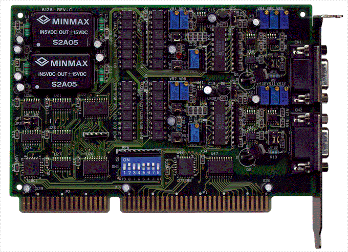
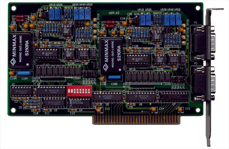
ACLD-7285
SUCHEN SIE DIE PASSENDE
INDUSTRIELLE LÖSUNG?
Entdecken Sie Embedded-, Kommunikations- und Automatisierungslösungen für Ihre Anwendung.
- Two Independent Analog Output Channels: Each channel operates independently with full isolation.
- High Isolation Protection: 5000 Vrms channel‑to‑channel and channel‑to‑system isolation ensures safety and noise immunity.
- 12‑bit Resolution: Double‑buffered DACs provide smooth, accurate analog output.
- Multiple Output Ranges:
- Bipolar: ±10 V, ±5 V
- Unipolar: 0–10 V, 0–5 V
- Current Sink: 0–20 mA, 4–20 mA
- High Throughput: Up to 16 kHz update rate per channel.
- Fast Settling Time: ≤ 30 µs typical.
- Integrated DC/DC Converters: Two onboard converters provide isolated power for each channel.
- Compact Half‑Size ISA Form Factor: 4‑layer PCB with dedicated ground plane for signal integrity.
- Software Compatibility: Fully register‑compatible with Advantech PCL‑728, minimizing migration effort.
- Software Triggered Output: Simplifies synchronization and control.
- Internal/External Reference Sources: Selectable precision internal −5 V/−10 V or external ±10 V reference.
- Comprehensive Software Support: Includes DOS C‑language library, Windows DLLs, and LabVIEW drivers.
- Industrial‑Grade Design: Surface‑mount components, single +5 V power supply, and wide operating temperature range.
- High Isolation Protection: 5000 Vrms channel‑to‑channel and channel‑to‑system isolation ensures safety and noise immunity.
- 12‑bit Resolution: Double‑buffered DACs provide smooth, accurate analog output.
- Multiple Output Ranges:
- Bipolar: ±10 V, ±5 V
- Unipolar: 0–10 V, 0–5 V
- Current Sink: 0–20 mA, 4–20 mA
- High Throughput: Up to 16 kHz update rate per channel.
- Fast Settling Time: ≤ 30 µs typical.
- Integrated DC/DC Converters: Two onboard converters provide isolated power for each channel.
- Compact Half‑Size ISA Form Factor: 4‑layer PCB with dedicated ground plane for signal integrity.
- Software Compatibility: Fully register‑compatible with Advantech PCL‑728, minimizing migration effort.
- Software Triggered Output: Simplifies synchronization and control.
- Internal/External Reference Sources: Selectable precision internal −5 V/−10 V or external ±10 V reference.
- Comprehensive Software Support: Includes DOS C‑language library, Windows DLLs, and LabVIEW drivers.
- Industrial‑Grade Design: Surface‑mount components, single +5 V power supply, and wide operating temperature range.
Comprehensive Product Summary: ADLINK ACL‑6128 Isolated 2‑Channel 12‑bit Analog Output ISA Card
### 1. Product Overview
- Product Name: ACL‑6128
- Model: ACL‑6128
- Series: NuDAQ ISA‑Bus Analog Output Series
- Article Number: 91‑11002‑011 (also referenced as 91‑11002‑001)
- Manufacturer: ADLINK Technology Inc.
- Manufacturer Address: 9F, No.166 Jian Yi Road, Chungho City, Taipei, Taiwan, R.O.C.
- Telephone: +886‑2‑8226‑5877
- Fax: +886‑2‑8226‑5717 / +886‑2‑8226‑5729 (Sales)
- Website: [www.adlinktech.com](http://www.adlinktech.com)
- Product Status: End‑of‑Life (EOL) as of January 22, 2003 (EOL No. 20030122‑008)
- Suggested Replacement: ADLINK PCI‑6308V
The ADLINK ACL‑6128 is a 2‑channel isolated analog output card designed for IBM PC/AT and compatible systems. It provides high‑precision 12‑bit digital‑to‑analog conversion with galvanic isolation, supporting both voltage and current output modes. The card is part of ADLINK’s NuDAQ family of ISA‑bus data acquisition products and was engineered for industrial control, signal generation, and instrumentation applications.
### 2. Key Features
- Two Independent Analog Output Channels: Each channel operates independently with full isolation.
- High Isolation Protection: 5000 Vrms channel‑to‑channel and channel‑to‑system isolation ensures safety and noise immunity.
- 12‑bit Resolution: Double‑buffered DACs provide smooth, accurate analog output.
- Multiple Output Ranges:
- Bipolar: ±10 V, ±5 V
- Unipolar: 0–10 V, 0–5 V
- Current Sink: 0–20 mA, 4–20 mA
- High Throughput: Up to 16 kHz update rate per channel.
- Fast Settling Time: ≤ 30 µs typical.
- Integrated DC/DC Converters: Two onboard converters provide isolated power for each channel.
- Compact Half‑Size ISA Form Factor: 4‑layer PCB with dedicated ground plane for signal integrity.
- Software Compatibility: Fully register‑compatible with Advantech PCL‑728, minimizing migration effort.
- Software Triggered Output: Simplifies synchronization and control.
- Internal/External Reference Sources: Selectable precision internal −5 V/−10 V or external ±10 V reference.
- Comprehensive Software Support: Includes DOS C‑language library, Windows DLLs, and LabVIEW drivers.
- Industrial‑Grade Design: Surface‑mount components, single +5 V power supply, and wide operating temperature range.
### 3. Technical Specifications
Analog Output (D/A):
- Channels: 2 isolated, independently configurable
- Resolution: 12 bits, double‑buffered
- Throughput: 16 kHz per channel
- Settling Time: ≤ 30 µs
- Output Ranges (jumper‑selectable):
- Bipolar: ±10 V, ±5 V
- Unipolar: 0–10 V, 0–5 V
- Current Sink: 0–20 mA, 4–20 mA
- Reference Voltage:
- Internal: −5 V and −10 V precision sources
- External: DC/AC ±10 V max (via REF.IN pin)
- Output Drive Current: ±5 mA
- Current Loop Excitation Voltage: +8 V (min) to +36 V (max)
- Isolation Voltage: ≥ 500 V DC (spec sheet) / 5000 Vrms (manual)
- Converter Type: AD7541 or equivalent
- Accuracy: ±0.012 % of full‑scale range
- Linearity: ±½ LSB
- Trigger Mode: Software trigger
- Data Transfer: Program control
- Temperature Coefficient: 5 ppm typical, 15 ppm max
General:
- Bus Interface: PC/AT ISA bus
- Connectors: Two 9‑pin D‑type female connectors (CN1, CN2)
- Power Requirement: +5 V @ 780 mA typical (1 A max)
- Dimensions: 163 mm (L) × 107 mm (W) (approx. 155 × 89 mm in EOL notice)
- Operating Temperature: 0 °C – 55 °C
- Storage Temperature: −20 °C – 70 °C
- Humidity: 5 – 95 % RH, non‑condensing
- PCB: 4‑layer with ground plane
- Isolation Components: Dual DC/DC converters and opto‑isolators
### 4. Functionality
The ACL‑6128 converts digital data from the host PC into isolated analog voltage or current outputs. Each channel includes a 12‑bit DAC with double buffering to ensure glitch‑free updates. The card supports both voltage and current output modes, selectable via onboard jumpers. Internal precision reference voltages (−5 V or −10 V) or external references can be used depending on application requirements.
Typical Use Cases:
- Arbitrary waveform generation
- Programmable voltage or current source
- Servo and actuator control
- Process control and instrumentation
- Relay and valve control
- Analog signal simulation for testing and calibration
Compatibility:
- Hardware: IBM PC/AT and compatible ISA systems
- Software: Compatible with ADLINK NuDAQ libraries, DOS, Windows 95/98/NT, and LabVIEW environments
- Register‑level compatibility with Advantech PCL‑728
### 5. Components & Accessories
Included Items:
- ACL‑6128 2‑channel isolated analog output card
- ADLINK CD containing drivers, libraries, and documentation
- Printed User’s Manual
Connectors:
- CN1 (Channel 1): 9‑pin D‑type female
- CN2 (Channel 2): 9‑pin D‑type female
Pin Assignments (per channel):
- Pin 1: V.OUT (Analog Voltage Output)
- Pin 2: A.GND (Analog Ground)
- Pin 3: REF.IN (Reference Voltage Input)
- Pin 4: A.GND
- Pin 5: A.GND
- Pin 6: A.GND
- Pin 7: I.SINK (Current Sink Output)
- Pin 8: +15 V (Auxiliary Power Output)
- Pin 9: A.GND
Optional Accessories:
- External reference voltage source (±10 V max)
- Shielded analog cables
- Terminal boards for signal breakout
### 6. Installation & Setup
System Requirements:
- IBM PC/AT or compatible computer with available ISA slot
- +5 V DC power supply (from system bus)
- Operating environment within 0–55 °C
Installation Steps:
1. Unpack the card in an ESD‑safe environment using a grounded wrist strap.
2. Verify no shipping damage and ensure all ICs are properly seated.
3. Insert the card into an available ISA slot.
4. Configure base I/O address using DIP switch SW1 (default: 2C0h).
- Address range: 200h – 3F0h (16 consecutive I/O addresses).
5. Set reference source (internal/external) via jumpers JP4 (CH1) and JP8 (CH2).
6. Select internal reference voltage (−5 V or −10 V) using JP3 (CH1) and JP7 (CH2).
7. Configure output range (unipolar/bipolar) using JP1/JP5 (CH1) and JP2/JP9 (CH2).
8. For current sink mode, set JP6 (CH1) and JP10 (CH2) to 0–20 mA or 4–20 mA.
9. Connect output signals to external devices via CN1/CN2.
10. Install software drivers and libraries from the ADLINK CD.
Signal Connection Examples:
- Voltage Output: Connect V.OUT to load input, A.GND to load ground.
- Current Sink: Connect I.SINK to load, return to external power supply or +15 V output if floating load.
- Floating Load: Use onboard +15 V output when no external supply is available.
### 7. Performance & Capabilities
- Update Rate: 16 kHz per channel (software‑triggered)
- Resolution: 12 bits (4096 discrete levels)
- Accuracy: ±0.012 % FSR
- Linearity: ±½ LSB
- Settling Time: ≤ 30 µs to 0.01 % FSR
- Output Drive: ±5 mA
- Isolation: 500 V DC (spec) / 5000 Vrms (manual)
- Temperature Drift: 5 ppm typical, 15 ppm max
- Power Consumption: +5 V @ 780 mA typical, 1 A max
Limitations:
- ISA bus interface limits data throughput compared to modern PCI/PCIe cards.
- Software‑triggered only (no hardware trigger or DMA).
- End‑of‑Life product; replacement recommended (PCI‑6308V).
### 8. Standards & Compliance
- Bus Standard: ISA (Industry Standard Architecture)
- Isolation Standard: 5000 Vrms channel‑to‑channel and channel‑to‑system
- Environmental: 0–55 °C operating, −20–70 °C storage, 5–95 % RH non‑condensing
- Safety: Designed for industrial environments with galvanic isolation
- Regulatory Compliance: Manufactured under ADLINK quality management system; conforms to internal reliability and safety standards applicable at time of production (1995–2000).
- EOL Compliance: Official End‑of‑Life notice issued January 22 2003 (EOL No. 20030122‑008).
### 9. Additional Information
Calibration:
- Twelve variable resistors (VR1–VR12) allow fine calibration of internal references, gain, and offsets.
- CH1: VR1–VR6
- CH2: VR7–VR12
- Test Points: TP1 (CH1), TP2 (CH2) for voltage measurement.
- Calibration covers internal reference (−5 V/−10 V), unipolar/bipolar gain and offset, and current sink offset (4 mA).
Software Support:
- DOS Library: C‑language functions for initialization and D/A conversion.
- `_6128_Initial(int card_number, int base_address)`
- `_6128_Switch_Card_No(int card_number)`
- `_6128_DA(int da_ch_no, unsigned int da_data)`
- Windows DLL: ACLS‑DLL2 for Windows 3.1/95/98/NT (supports VC++, VB, Delphi).
- LabVIEW Driver: ACLS‑LVIEW for Windows 95/98/NT integration.
- Programming Example: 6128IO.C demonstrates low‑level I/O control.
Maintenance & Service:
- ADLINK provides technical support via dedicated email channels:
- General Service: service@adlink.com.tw
- NuDAQ Technical: nudaq@adlink.com.tw
- NuDAM Support: nudam@adlink.com.tw
- Software: sw@adlink.com.tw
- Calibration and repair services available through ADLINK service centers.
Warranty:
- Standard limited warranty: 1 year from date of purchase.
- Coverage: Defects in materials and workmanship.
- Exclusions: Damage from misuse, modification, or operation beyond specifications.
- Remedy: Repair or replacement at ADLINK’s discretion.
- Return Policy: Prepaid, insured shipment required; proof of purchase necessary.
Product Lifecycle:
- EOL Publication Date: January 22 2003
- Reason for EOL: Material discontinuation, market phase‑out, and replacement by PCI‑based models.
- Replacement Product: ADLINK PCI‑6308V (PCI‑bus 12‑bit analog output card).
- Last‑Time Buy: No remaining stock; new orders non‑cancelable.
Documentation:
- User’s Guide Revision 2.22 (June 29 2000)
- Contains detailed jumper settings, calibration procedures, and programming references.
- Proprietary information © 1995–2000 ADLINK Technology Inc.
### Summary
The ADLINK ACL‑6128 is a robust, isolated 2‑channel 12‑bit analog output card for ISA‑bus systems, designed for industrial and laboratory applications requiring precise voltage or current generation. Its dual isolated DACs, flexible output ranges, and internal/external reference options make it suitable for control, simulation, and signal generation tasks. With 5000 Vrms isolation, 16 kHz throughput, and ±0.012 % FSR accuracy, it delivers reliable performance in harsh environments. Although discontinued, the ACL‑6128 remains a reference design for isolated analog output solutions and can be replaced by the PCI‑6308V for modern systems.
Keywords: ADLINK ACL‑6128, 12‑bit DAC, isolated analog output, ISA card, 2‑channel D/A converter, ±10 V output, 4–20 mA current loop, industrial control, NuDAQ, PCI‑6308V replacement, calibration, EOL 2003.

### 1. Product Overview
- Product Name: ACL‑6128
- Model: ACL‑6128
- Series: NuDAQ ISA‑Bus Analog Output Series
- Article Number: 91‑11002‑011 (also referenced as 91‑11002‑001)
- Manufacturer: ADLINK Technology Inc.
- Manufacturer Address: 9F, No.166 Jian Yi Road, Chungho City, Taipei, Taiwan, R.O.C.
- Telephone: +886‑2‑8226‑5877
- Fax: +886‑2‑8226‑5717 / +886‑2‑8226‑5729 (Sales)
- Website: [www.adlinktech.com](http://www.adlinktech.com)
- Product Status: End‑of‑Life (EOL) as of January 22, 2003 (EOL No. 20030122‑008)
- Suggested Replacement: ADLINK PCI‑6308V
The ADLINK ACL‑6128 is a 2‑channel isolated analog output card designed for IBM PC/AT and compatible systems. It provides high‑precision 12‑bit digital‑to‑analog conversion with galvanic isolation, supporting both voltage and current output modes. The card is part of ADLINK’s NuDAQ family of ISA‑bus data acquisition products and was engineered for industrial control, signal generation, and instrumentation applications.
### 2. Key Features
- Two Independent Analog Output Channels: Each channel operates independently with full isolation.
- High Isolation Protection: 5000 Vrms channel‑to‑channel and channel‑to‑system isolation ensures safety and noise immunity.
- 12‑bit Resolution: Double‑buffered DACs provide smooth, accurate analog output.
- Multiple Output Ranges:
- Bipolar: ±10 V, ±5 V
- Unipolar: 0–10 V, 0–5 V
- Current Sink: 0–20 mA, 4–20 mA
- High Throughput: Up to 16 kHz update rate per channel.
- Fast Settling Time: ≤ 30 µs typical.
- Integrated DC/DC Converters: Two onboard converters provide isolated power for each channel.
- Compact Half‑Size ISA Form Factor: 4‑layer PCB with dedicated ground plane for signal integrity.
- Software Compatibility: Fully register‑compatible with Advantech PCL‑728, minimizing migration effort.
- Software Triggered Output: Simplifies synchronization and control.
- Internal/External Reference Sources: Selectable precision internal −5 V/−10 V or external ±10 V reference.
- Comprehensive Software Support: Includes DOS C‑language library, Windows DLLs, and LabVIEW drivers.
- Industrial‑Grade Design: Surface‑mount components, single +5 V power supply, and wide operating temperature range.
### 3. Technical Specifications
Analog Output (D/A):
- Channels: 2 isolated, independently configurable
- Resolution: 12 bits, double‑buffered
- Throughput: 16 kHz per channel
- Settling Time: ≤ 30 µs
- Output Ranges (jumper‑selectable):
- Bipolar: ±10 V, ±5 V
- Unipolar: 0–10 V, 0–5 V
- Current Sink: 0–20 mA, 4–20 mA
- Reference Voltage:
- Internal: −5 V and −10 V precision sources
- External: DC/AC ±10 V max (via REF.IN pin)
- Output Drive Current: ±5 mA
- Current Loop Excitation Voltage: +8 V (min) to +36 V (max)
- Isolation Voltage: ≥ 500 V DC (spec sheet) / 5000 Vrms (manual)
- Converter Type: AD7541 or equivalent
- Accuracy: ±0.012 % of full‑scale range
- Linearity: ±½ LSB
- Trigger Mode: Software trigger
- Data Transfer: Program control
- Temperature Coefficient: 5 ppm typical, 15 ppm max
General:
- Bus Interface: PC/AT ISA bus
- Connectors: Two 9‑pin D‑type female connectors (CN1, CN2)
- Power Requirement: +5 V @ 780 mA typical (1 A max)
- Dimensions: 163 mm (L) × 107 mm (W) (approx. 155 × 89 mm in EOL notice)
- Operating Temperature: 0 °C – 55 °C
- Storage Temperature: −20 °C – 70 °C
- Humidity: 5 – 95 % RH, non‑condensing
- PCB: 4‑layer with ground plane
- Isolation Components: Dual DC/DC converters and opto‑isolators
### 4. Functionality
The ACL‑6128 converts digital data from the host PC into isolated analog voltage or current outputs. Each channel includes a 12‑bit DAC with double buffering to ensure glitch‑free updates. The card supports both voltage and current output modes, selectable via onboard jumpers. Internal precision reference voltages (−5 V or −10 V) or external references can be used depending on application requirements.
Typical Use Cases:
- Arbitrary waveform generation
- Programmable voltage or current source
- Servo and actuator control
- Process control and instrumentation
- Relay and valve control
- Analog signal simulation for testing and calibration
Compatibility:
- Hardware: IBM PC/AT and compatible ISA systems
- Software: Compatible with ADLINK NuDAQ libraries, DOS, Windows 95/98/NT, and LabVIEW environments
- Register‑level compatibility with Advantech PCL‑728
### 5. Components & Accessories
Included Items:
- ACL‑6128 2‑channel isolated analog output card
- ADLINK CD containing drivers, libraries, and documentation
- Printed User’s Manual
Connectors:
- CN1 (Channel 1): 9‑pin D‑type female
- CN2 (Channel 2): 9‑pin D‑type female
Pin Assignments (per channel):
- Pin 1: V.OUT (Analog Voltage Output)
- Pin 2: A.GND (Analog Ground)
- Pin 3: REF.IN (Reference Voltage Input)
- Pin 4: A.GND
- Pin 5: A.GND
- Pin 6: A.GND
- Pin 7: I.SINK (Current Sink Output)
- Pin 8: +15 V (Auxiliary Power Output)
- Pin 9: A.GND
Optional Accessories:
- External reference voltage source (±10 V max)
- Shielded analog cables
- Terminal boards for signal breakout
### 6. Installation & Setup
System Requirements:
- IBM PC/AT or compatible computer with available ISA slot
- +5 V DC power supply (from system bus)
- Operating environment within 0–55 °C
Installation Steps:
1. Unpack the card in an ESD‑safe environment using a grounded wrist strap.
2. Verify no shipping damage and ensure all ICs are properly seated.
3. Insert the card into an available ISA slot.
4. Configure base I/O address using DIP switch SW1 (default: 2C0h).
- Address range: 200h – 3F0h (16 consecutive I/O addresses).
5. Set reference source (internal/external) via jumpers JP4 (CH1) and JP8 (CH2).
6. Select internal reference voltage (−5 V or −10 V) using JP3 (CH1) and JP7 (CH2).
7. Configure output range (unipolar/bipolar) using JP1/JP5 (CH1) and JP2/JP9 (CH2).
8. For current sink mode, set JP6 (CH1) and JP10 (CH2) to 0–20 mA or 4–20 mA.
9. Connect output signals to external devices via CN1/CN2.
10. Install software drivers and libraries from the ADLINK CD.
Signal Connection Examples:
- Voltage Output: Connect V.OUT to load input, A.GND to load ground.
- Current Sink: Connect I.SINK to load, return to external power supply or +15 V output if floating load.
- Floating Load: Use onboard +15 V output when no external supply is available.
### 7. Performance & Capabilities
- Update Rate: 16 kHz per channel (software‑triggered)
- Resolution: 12 bits (4096 discrete levels)
- Accuracy: ±0.012 % FSR
- Linearity: ±½ LSB
- Settling Time: ≤ 30 µs to 0.01 % FSR
- Output Drive: ±5 mA
- Isolation: 500 V DC (spec) / 5000 Vrms (manual)
- Temperature Drift: 5 ppm typical, 15 ppm max
- Power Consumption: +5 V @ 780 mA typical, 1 A max
Limitations:
- ISA bus interface limits data throughput compared to modern PCI/PCIe cards.
- Software‑triggered only (no hardware trigger or DMA).
- End‑of‑Life product; replacement recommended (PCI‑6308V).
### 8. Standards & Compliance
- Bus Standard: ISA (Industry Standard Architecture)
- Isolation Standard: 5000 Vrms channel‑to‑channel and channel‑to‑system
- Environmental: 0–55 °C operating, −20–70 °C storage, 5–95 % RH non‑condensing
- Safety: Designed for industrial environments with galvanic isolation
- Regulatory Compliance: Manufactured under ADLINK quality management system; conforms to internal reliability and safety standards applicable at time of production (1995–2000).
- EOL Compliance: Official End‑of‑Life notice issued January 22 2003 (EOL No. 20030122‑008).
### 9. Additional Information
Calibration:
- Twelve variable resistors (VR1–VR12) allow fine calibration of internal references, gain, and offsets.
- CH1: VR1–VR6
- CH2: VR7–VR12
- Test Points: TP1 (CH1), TP2 (CH2) for voltage measurement.
- Calibration covers internal reference (−5 V/−10 V), unipolar/bipolar gain and offset, and current sink offset (4 mA).
Software Support:
- DOS Library: C‑language functions for initialization and D/A conversion.
- `_6128_Initial(int card_number, int base_address)`
- `_6128_Switch_Card_No(int card_number)`
- `_6128_DA(int da_ch_no, unsigned int da_data)`
- Windows DLL: ACLS‑DLL2 for Windows 3.1/95/98/NT (supports VC++, VB, Delphi).
- LabVIEW Driver: ACLS‑LVIEW for Windows 95/98/NT integration.
- Programming Example: 6128IO.C demonstrates low‑level I/O control.
Maintenance & Service:
- ADLINK provides technical support via dedicated email channels:
- General Service: service@adlink.com.tw
- NuDAQ Technical: nudaq@adlink.com.tw
- NuDAM Support: nudam@adlink.com.tw
- Software: sw@adlink.com.tw
- Calibration and repair services available through ADLINK service centers.
Warranty:
- Standard limited warranty: 1 year from date of purchase.
- Coverage: Defects in materials and workmanship.
- Exclusions: Damage from misuse, modification, or operation beyond specifications.
- Remedy: Repair or replacement at ADLINK’s discretion.
- Return Policy: Prepaid, insured shipment required; proof of purchase necessary.
Product Lifecycle:
- EOL Publication Date: January 22 2003
- Reason for EOL: Material discontinuation, market phase‑out, and replacement by PCI‑based models.
- Replacement Product: ADLINK PCI‑6308V (PCI‑bus 12‑bit analog output card).
- Last‑Time Buy: No remaining stock; new orders non‑cancelable.
Documentation:
- User’s Guide Revision 2.22 (June 29 2000)
- Contains detailed jumper settings, calibration procedures, and programming references.
- Proprietary information © 1995–2000 ADLINK Technology Inc.
### Summary
The ADLINK ACL‑6128 is a robust, isolated 2‑channel 12‑bit analog output card for ISA‑bus systems, designed for industrial and laboratory applications requiring precise voltage or current generation. Its dual isolated DACs, flexible output ranges, and internal/external reference options make it suitable for control, simulation, and signal generation tasks. With 5000 Vrms isolation, 16 kHz throughput, and ±0.012 % FSR accuracy, it delivers reliable performance in harsh environments. Although discontinued, the ACL‑6128 remains a reference design for isolated analog output solutions and can be replaced by the PCI‑6308V for modern systems.
Keywords: ADLINK ACL‑6128, 12‑bit DAC, isolated analog output, ISA card, 2‑channel D/A converter, ±10 V output, 4–20 mA current loop, industrial control, NuDAQ, PCI‑6308V replacement, calibration, EOL 2003.

-
20030122-008(ACL-6128).pdf
Manual
-
A6128 Manual.PDF
Manual