Comprehensive Product Summary: ADLINK LPCI‑9112G Low‑Profile PCI Multi‑Function Data Acquisition Card
### 1. Product Overview
Product Name: LPCI‑9112G
Model Number: LPCI‑9112G
Series: PCI‑9112 / LPCI‑9112 Multi‑Function DAQ Series
Article Number: LPCI‑9112G
Manufacturer: ADLINK Technology Inc.
Product Type: Low‑Profile PCI Multi‑Function Data Acquisition (DAQ) Card
Bus Interface: Universal PCI (3.3 V / 5 V compatible)
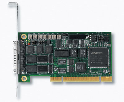
Form Factor: MD1 Low‑Profile PCI Card (120 mm × 65 mm)
The ADLINK LPCI‑9112G is a compact, high‑performance, low‑profile data acquisition card designed for industrial, laboratory, and embedded measurement systems. It is the low‑profile variant of the PCI‑9112, offering identical functionality in a smaller MD1 form factor suitable for space‑constrained systems. The card provides 16 single‑ended or 8 differential analog inputs, two 12‑bit analog outputs, 16 digital inputs, 16 digital outputs, and a 16‑bit general‑purpose timer/counter. It supports a maximum sampling rate of 110 kS/s with 12‑bit resolution and includes a DC/DC converter for stable analog power.
### 2. Key Features
- High‑Resolution Analog Input:
16 single‑ended or 8 differential analog input channels with 12‑bit resolution and up to 110 kS/s sampling rate.
- Flexible Input Configuration:
Software‑selectable bipolar and unipolar input ranges with programmable gains (×0.5, ×1, ×2, ×4, ×8).
- Dual Analog Outputs:
Two 12‑bit D/A channels with programmable output ranges (0–5 V, 0–10 V, or external reference), ±5 mA drive, and 30 µs settling time.
- Digital I/O:
16 TTL‑compatible digital inputs and 16 TTL‑compatible digital outputs for control and monitoring applications.
- Timer/Counter:
One 16‑bit general‑purpose counter/timer (Intel 8254 compatible) with a 2 MHz base clock and external clock input up to 10 MHz.
- Low‑Profile Design:
MD1‑size (120 × 65 mm) PCI card suitable for compact industrial PCs and embedded systems.
- Universal PCI Support:
Compatible with both 3.3 V and 5 V PCI slots, ensuring broad system compatibility.
- Automatic Channel Scanning:
Hardware‑based auto‑scan for sequential analog input sampling.
- Noise Reduction:
Differential input mode for improved common‑mode noise rejection.
- On‑Board DC/DC Converter:
Provides isolated and stable analog power for improved measurement accuracy.
- Plug‑and‑Play Configuration:
Fully PCI‑compliant with automatic resource allocation (IRQ, I/O base address).
- Comprehensive Software Support:
Includes drivers, DLLs, and libraries for DOS, Windows 95/98/NT, and supports LabVIEW, DASYLab, HP‑VEE, and InTouch.
### 3. Technical Specifications
Analog Input (A/D):
- Channels: 16 SE or 8 DIFF
- Resolution: 12 bits
- Conversion Time: 8 µs
- Max Sampling Rate: 110 kS/s
- Input Coupling: DC
- Input Impedance: 1 GΩ
- Overvoltage Protection: ±35 V continuous
- Input Ranges (software‑selectable):
- Bipolar: ±10 V, ±5 V, ±2.5 V, ±1.25 V, ±0.625 V
- Unipolar: 0–10 V, 0–5 V, 0–2.5 V, 0–1.25 V
- Accuracy:
- Gain 0.5–1: ±0.01 % FSR ± 1 LSB
- Gain 2–4: ±0.02 % FSR ± 1 LSB
- Gain 8: ±0.04 % FSR ± 1 LSB
- Trigger Modes: Software, Pacer (Timer), External
- Data Transfer: Programmed I/O, Interrupt, Bus‑Mastering DMA
Analog Output (D/A):
- Channels: 2 voltage outputs
- Resolution: 12 bits
- Output Ranges: 0–10 V, 0–5 V, or 0–EXTREF (software‑selectable)
- Output Drive: ±5 mA max
- Settling Time: 30 µs to 0.5 LSB
- Converter Type: AD7541 or equivalent
- Data Transfer: Programmed I/O
Digital I/O:
- Inputs: 16 TTL/DTL‑compatible
- Outputs: 16 TTL/DTL‑compatible
- Logic Levels:
- Input Low ≤ 0.8 V, High ≥ 2.0 V
- Output Low ≤ 0.4 V @ 8 mA sink, High ≥ 2.4 V @ 0.4 mA source
- Data Transfer: Programmed I/O
Timer/Counter:
- Channels: 1 (16‑bit)
- Base Clock: 2 MHz internal, external up to 10 MHz
- Compatibility: 8253/8254 TTL
- Modes: 0–5 (programmable)
Physical & Environmental:
- Dimensions: 120 mm × 65 mm (LPCI‑9112)
- Weight: Approx. 100 g
- Operating Temperature: 0 °C to 60 °C
- Storage Temperature: –20 °C to 80 °C
- Humidity: 5 % to 95 % RH (non‑condensing)
- I/O Connector: 68‑pin VHDCI (SCSI‑3 type)
- Power Requirements:
- +5 V @ 500 mA typical
- +12 V @ 110 mA typical
### 4. Functionality
The LPCI‑9112G performs multi‑function data acquisition through its integrated A/D, D/A, DIO, and timer subsystems.
Operation Principles:
- Analog Input: The onboard 12‑bit successive‑approximation ADC (Burr‑Brown ADS774) samples up to 110 kS/s. Input channels can be configured as 16 single‑ended or 8 differential. Programmable gain amplifiers allow flexible voltage range selection.
- Analog Output: Two 12‑bit DACs (AD7541) provide precise voltage generation for control or waveform output.
- Digital I/O: TTL‑compatible lines enable monitoring and control of external devices.
- Timer/Counter: The integrated 8254 timer provides pacer triggers for A/D sampling or can be used for event counting and frequency generation.
Use Cases & Applications:
- Industrial process monitoring and control
- Laboratory instrumentation and data logging
- Automated test systems
- Energy management and environmental monitoring
- Signal analysis and waveform generation
- Event counting and timing applications
Compatibility:
- Universal PCI (3.3 V/5 V)
- Supported OS: DOS, Windows 95/98/NT
- Software Integration: LabVIEW, DASYLab, HP‑VEE, InTouch, DAQBench, PCIS‑DASK
### 5. Components & Accessories
Included:
- LPCI‑9112G DAQ Card
- Software & Utility CD (drivers, DLLs, C libraries, utilities)
- User Manual
Optional Termination Boards:
- DIN‑68S/1M: 68‑pin SCSI‑II DIN‑rail termination board with 1 m ACL‑10568 cable (for LPCI‑9112)
- DIN‑37D: 37‑pin D‑sub DIN‑rail termination board with 1 m ACL‑10137 cable (for PCI‑9112)
- DIN‑20P: 20‑pin ribbon DIN‑rail termination board with 1 m ACL‑10120 cable
- ACLD‑9137/9138: General‑purpose termination boards with 37‑pin D‑sub connectors
- ACLD‑8125: Termination board with CJC temperature sensor and 37‑pin D‑sub connector
- ACLD‑9182A: 16‑channel isolated digital input board
- ACLD‑9185: 16‑channel relay output board
- ACLD‑9188: General‑purpose termination board with dual 20‑pin ribbon and 37‑pin D‑sub connectors
Connectors:
- CN1: Digital Input (20‑pin IDC)
- CN2: Digital Output (20‑pin IDC)
- CN3: Analog I/O & Timer (68‑pin VHDCI for LPCI‑9112)
### 6. Installation & Setup
System Requirements:
- PCI slot (3.3 V or 5 V)
- Compatible PC running DOS or Windows 95/98/NT
Installation Steps:
1. Power off the PC and insert the LPCI‑9112G into an available PCI slot.
2. Power on the system; the card is automatically detected by the BIOS (Plug and Play).
3. Install drivers from the ADLINK Software Utility CD.
4. Configure the card using the 9112UTIL.EXE utility for calibration and testing.
Configuration Options:
- Analog Input Mode: 16 SE or 8 DIFF (selectable via software or jumpers JP1/JP5).
- Clock Source: Internal 2 MHz or external clock input (JP2).
- D/A Reference Voltage: Internal (–5 V or –10 V) or external (JP3/JP4).
- Trigger Modes: Software, Timer Pacer, External.
Calibration:
- Factory‑calibrated; user adjustment via VR potentiometers (VR1–VR7) for A/D offset, gain, and D/A reference.
- Software calibration utility included for automated adjustment.
### 7. Performance & Capabilities
- A/D Sampling Rate: Up to 110 kS/s (12‑bit)
- A/D Conversion Time: 8 µs
- A/D FIFO: 1 k samples (PCI‑9112) / 2 k samples (cPCI‑9112)
- D/A Settling Time: 30 µs to 0.5 LSB
- Timer Resolution: 16 bits (2 MHz base clock)
- DMA Transfer Rate: Bus‑mastering PCI DMA for high‑speed data transfer
- Accuracy: ±0.01 % FSR to ±0.04 % FSR depending on gain
- Noise Rejection: Differential mode for high CMRR
- Power Efficiency: Low power consumption (≤ 3 W typical)
Limitations:
- 12‑bit resolution may not suit ultra‑high‑precision applications.
- Single A/D converter limits simultaneous multi‑channel sampling.
- Maximum sampling rate 110 kS/s shared across channels.
### 8. Standards & Compliance
- Bus Interface: PCI 2.1 compliant (32‑bit, 33 MHz)
- Voltage Compatibility: Universal PCI (3.3 V / 5 V)
- Digital Logic Levels: TTL/DTL compatible
- Environmental Compliance: Operating 0–60 °C, non‑condensing humidity 5–95 %
- Safety & EMC: Designed for industrial environments (CE and FCC Class A compliance typical for ADLINK DAQ cards)
- RoHS Compliance: Yes (for modern production versions)
### 9. Additional Information
Warranty: 1‑year limited manufacturer warranty against defects in materials and workmanship.
Support & Service:
- Technical Support: nudaq@adlink.com.tw
- Sales & Service: service@adlink.com.tw
- Website: [www.adlinktech.com](https://www.adlinktech.com)
- Phone: +886‑2‑82265877 Fax: +886‑2‑82265717
- Address: 9F, No. 166, Jian Yi Road, Chungho City, Taipei 235, Taiwan, R.O.C.
Maintenance:
- Periodic re‑calibration recommended every 6–12 months (depending on environment).
- Avoid exposure to excessive vibration or temperature fluctuations.
Software Utilities & Libraries:
- 9112UTIL.EXE: Configuration, calibration, and functional testing utility.
- C/C++ Library & DLLs: 29 API functions for A/D, D/A, DIO, and timer operations.
- Supported Languages: C/C++, Visual Basic, LabVIEW, DASYLab.
- Demo Programs: AD_DEMO1–7, DA_DEMO, DIO_DEMO for DOS; 9112DMA.EXE, 9112INT.EXE, 9112UTIL.EXE for Windows.
Calibration Controls (VR Adjustments):
- VR1 – A/D bipolar offset
- VR2 – A/D full‑scale adjust
- VR3 – D/A CH1 full‑scale
- VR4 – D/A CH2 full‑scale
- VR5 – A/D unipolar offset
- VR6 – D/A reference voltage
- VR7 – A/D PGA offset
Ordering Information:
- LPCI‑9112: 16‑CH, 12‑bit, 110 kS/s Low‑Profile Multi‑Function DAQ Card
- PCI‑9112: Standard PCI version (175 × 107 mm)
### Summary
The ADLINK LPCI‑9112G is a robust, low‑profile, multi‑function PCI data acquisition card engineered for precision measurement and control in industrial and laboratory environments. It combines 12‑bit analog input and output, digital I/O, and timing functions in a compact MD1 form factor. With universal PCI compatibility, programmable input ranges, and comprehensive software support, it provides a versatile and cost‑effective solution for data logging, process automation, and test applications. Its stable DC/DC‑isolated analog power, hardware auto‑scan, and bus‑mastering DMA ensure reliable, high‑speed performance in demanding embedded systems.


 SUCHEN SIE DIE PASSENDE
 05-21.pdf
PDF Catalog
05-21.pdf
PDF Catalog
 LPCI-9112_Datasheet_1.pdf
PDF Catalog
LPCI-9112_Datasheet_1.pdf
PDF Catalog
 P9112 Manual.PDF
Manual
P9112 Manual.PDF
Manual

l_rgb_96dpi_500x500.jpg)
_up_rgb_96dpi_500x500.jpg)