WD-DASK
SUCHEN SIE DIE PASSENDE
INDUSTRIELLE LÖSUNG?
Entdecken Sie Embedded-, Kommunikations- und Automatisierungslösungen für Ihre Anwendung.
- High-Speed Sampling: Up to 20 MS/s simultaneous sampling across four channels.
- Resolution: 12-bit A/D conversion (10-bit for PCI-9810 variant).
- Simultaneous Sampling: Four independent A/D converters allow true simultaneous acquisition.
- Input Ranges: Bipolar ±1 V or ±5 V, selectable via solder jumpers.
- Input Impedance Options: 50 Ω, 1.25 kΩ, or 15 MΩ (solder-selectable).
- FIFO Buffer: 32k-sample onboard FIFO (128k-sample for PCI-9812A).
- Triggering: Supports software, analog, and external digital triggers with multiple modes (pre-, post-, middle-, delay-, and software-trigger).
- Clock Sources: Internal 40 MHz time base, external digital clock (TTL), or external sine wave clock (AC-coupled).
- Bus Interface: 32-bit PCI bus with bus-mastering DMA for high-speed data transfer.
- Connectors: Five BNC connectors (four analog inputs + one external sine clock) and one 10-pin digital I/O header.
- Software Support: Comprehensive C/C++ libraries, ActiveX controls, LabVIEW drivers, and DASYLab compatibility.
- Applications: Ideal for high-speed data acquisition in DSP, FFT, imaging, ultrasonic, and vibration testing systems.
- Resolution: 12-bit A/D conversion (10-bit for PCI-9810 variant).
- Simultaneous Sampling: Four independent A/D converters allow true simultaneous acquisition.
- Input Ranges: Bipolar ±1 V or ±5 V, selectable via solder jumpers.
- Input Impedance Options: 50 Ω, 1.25 kΩ, or 15 MΩ (solder-selectable).
- FIFO Buffer: 32k-sample onboard FIFO (128k-sample for PCI-9812A).
- Triggering: Supports software, analog, and external digital triggers with multiple modes (pre-, post-, middle-, delay-, and software-trigger).
- Clock Sources: Internal 40 MHz time base, external digital clock (TTL), or external sine wave clock (AC-coupled).
- Bus Interface: 32-bit PCI bus with bus-mastering DMA for high-speed data transfer.
- Connectors: Five BNC connectors (four analog inputs + one external sine clock) and one 10-pin digital I/O header.
- Software Support: Comprehensive C/C++ libraries, ActiveX controls, LabVIEW drivers, and DASYLab compatibility.
- Applications: Ideal for high-speed data acquisition in DSP, FFT, imaging, ultrasonic, and vibration testing systems.
Comprehensive Product Summary – ADLINK PCI-9812
### 1. Product Overview
Product Name: PCI-9812
Model: PCI-9812
Series: NuDAQ PCI Data Acquisition Series
Article Number: PCI-9812
Manufacturer: ADLINK Technology Inc. (Taipei, Taiwan, R.O.C.)
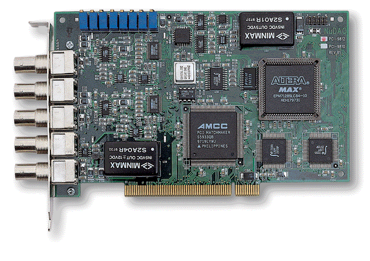
Product Type: 4-Channel, 12-bit, 20 MS/s Simultaneous-Sampling Analog Input PCI Data Acquisition Card
Related Models:
- PCI-9810: 10-bit, 20 MS/s, 32k-sample FIFO
- PCI-9812: 12-bit, 20 MS/s, 32k-sample FIFO
- PCI-9812A: 12-bit, 20 MS/s, 128k-sample FIFO
Product Description:
The ADLINK PCI-9812 is a high-performance PCI-bus analog-to-digital (A/D) acquisition card designed for simultaneous sampling of up to four single-ended analog input channels at a maximum rate of 20 million samples per second (20 MS/s). It features 12-bit resolution, a 32k-sample FIFO buffer, and supports multiple trigger modes and clock sources. The card is optimized for high-speed data acquisition in industrial, scientific, and military applications such as vibration analysis, ultrasonic measurement, image digitization, and automated test equipment (ATE).
### 2. Key Features
- High-Speed Sampling: Up to 20 MS/s simultaneous sampling across four channels.
- Resolution: 12-bit A/D conversion (10-bit for PCI-9810 variant).
- Simultaneous Sampling: Four independent A/D converters allow true simultaneous acquisition.
- Input Ranges: Bipolar ±1 V or ±5 V, selectable via solder jumpers.
- Input Impedance Options: 50 Ω, 1.25 kΩ, or 15 MΩ (solder-selectable).
- FIFO Buffer: 32k-sample onboard FIFO (128k-sample for PCI-9812A).
- Triggering: Supports software, analog, and external digital triggers with multiple modes (pre-, post-, middle-, delay-, and software-trigger).
- Clock Sources: Internal 40 MHz time base, external digital clock (TTL), or external sine wave clock (AC-coupled).
- Bus Interface: 32-bit PCI bus with bus-mastering DMA for high-speed data transfer.
- Connectors: Five BNC connectors (four analog inputs + one external sine clock) and one 10-pin digital I/O header.
- Software Support: Comprehensive C/C++ libraries, ActiveX controls, LabVIEW drivers, and DASYLab compatibility.
- Applications: Ideal for high-speed data acquisition in DSP, FFT, imaging, ultrasonic, and vibration testing systems.
### 3. Technical Specifications
Analog Input
- Channels: 4 single-ended
- Resolution: 12-bit (PCI-9812/9812A), 10-bit (PCI-9810)
- Sampling Rate: Up to 20 MS/s per channel (simultaneous)
- Input Range: ±1 V or ±5 V (bipolar)
- Input Impedance:
- 50 Ω (±1 V or ±5 V)
- 1.25 kΩ (±5 V only)
- 15 MΩ (±1 V only)
- Accuracy: ±1.5% typical at 25°C
- Differential Nonlinearity (DNL): ±0.4 LSB typical, ±1.0 LSB max
- Integral Nonlinearity (INL): ±1.9 LSB typical
- Input Coupling: DC
- Overvoltage Protection: ±10 V
FIFO Buffer
- 32k samples (PCI-9812, PCI-9810)
- 128k samples (PCI-9812A)
Triggering
- Sources: Software, analog (CH0–CH3), external digital (TTL)
- Modes: Software, pre-trigger, post-trigger, middle-trigger, delay-trigger
- Analog Trigger Sensitivity: 256 steps across full-scale range
- Digital Trigger Compatibility: 5 V TTL, minimum pulse width 25 ns
- Trigger Slope: Rising or falling edge
Clock Sources
- Internal Clock: 40 MHz oscillator (divisible by 2–1024)
- External Sine Clock: 300 kHz–40 MHz, 1.0–2.0 Vpp, 50 Ω AC-coupled
- External Digital Clock: 20 kHz–40 MHz, TTL-compatible, 50 Ω DC-coupled
Digital Input
- Channels: 3 TTL-compatible inputs
- Input Voltage:
- Low: 0–0.8 V
- High: 2.0–5.5 V
- Input Load: 10 kΩ pull-down resistors
- Overvoltage Protection: Diode clamping, -0.3 V to +5.3 V
General Specifications
- Bus Interface: 32-bit PCI, bus-mastering DMA
- Connectors:
- 5 × BNC (CH0–CH3, external sine clock)
- 10-pin ribbon header (digital I/O, external digital clock/trigger)
- Dimensions: 173 mm (L) × 108 mm (H)
- Operating Temperature: 0°C to 40°C
- Storage Temperature: -20°C to 70°C
- Humidity: 5–95% RH, non-condensing
- Power Requirements: +5 V @ 1.4 A typical (PCI-9812), 1.0 A typical (PCI-9812A)
### 4. Functionality
Operation Principle:
The PCI-9812 performs simultaneous sampling of four analog channels using four independent 12-bit A/D converters. The sampled data is temporarily stored in the onboard FIFO buffer before being transferred to host memory via bus-mastering DMA. The card supports both internal and external clock sources, as well as multiple trigger configurations for flexible acquisition control.
Use Cases & Applications:
- Vibration and acoustic analysis
- Ultrasonic and biomedical signal measurement
- Image digitization and CCD capture
- IF/baseband signal digitization
- Automated test equipment (ATE)
- High-speed DSP and FFT analysis
Compatibility:
- PCI 2.1 compliant
- Supported OS: MS-DOS, Windows 95/98/NT
- Software integration with LabVIEW, DASYLab, and ADLINK’s PCIS-DASK libraries
### 5. Components & Accessories
Included Items:
- PCI-9812/10 Data Acquisition Card
- 5 × BNC terminators
- ADLINK “All-in-One” Software CD (drivers, utilities, libraries)
- User’s Guide and installation documentation
Connectors:
- J1–J4: Analog input channels CH0–CH3 (BNC)
- J5: External sine wave clock input (BNC)
- JP1 (10-pin header):
- Pin 1: External digital clock
- Pin 3: External digital trigger
- Pins 5, 7, 9: Digital inputs DI0–DI2
- Even pins: Ground
Optional Accessories:
- Shielded BNC cables
- External clock sources
- Termination boards and calibration tools
### 6. Installation & Setup
Hardware Installation:
1. Power off the computer and remove the cover.
2. Insert the PCI-9812 into an available 32-bit PCI slot.
3. Secure the card with the mounting screw.
4. Reassemble and power on the system.
5. The card is plug-and-play; IRQ and I/O addresses are automatically assigned by BIOS.
Software Installation:
- Insert the ADLINK “All-in-One” CD.
- For Windows 95/98: Run `Setup.exe` and install the PCI-9812 driver and DLL.
- For DOS: Run `SETUP` from the `NuDAQPCI\9812\DOS` directory.
Configuration:
- Input range and impedance are set via solder jumpers (C0LO/C05V, etc.).
- External clock and trigger connections are made via BNC and JP1 headers.
- Software utilities (9812util.exe) assist with configuration, calibration, and testing.
### 7. Performance & Capabilities
Sampling Performance:
- 20 MS/s per channel (simultaneous)
- 12-bit resolution (4096 quantization levels)
- Throughput: up to 160 MB/s (4 channels × 20M × 2 bytes)
Data Transfer:
- Bus-mastering DMA for high-speed, low-latency data transfer
- Sustained PCI bandwidth: ~100 MB/s (peak 132 MB/s)
- FIFO buffering prevents data loss during high-speed bursts
Efficiency & Limitations:
- Continuous acquisition limited by PCI bandwidth and host memory
- 32k-sample FIFO limits full-rate acquisition duration when all channels active
- PCI-9812A (128k FIFO) recommended for extended high-speed capture
Dynamic Range & Accuracy:
- ±1.5% gain error typical
- ±0.4 LSB DNL, ±1.9 LSB INL
- Stable operation across 0–40°C
### 8. Standards & Compliance
- Bus Interface: PCI Local Bus Specification Rev. 2.1 compliant
- Signal Compatibility: TTL-level digital I/O
- Safety & Environmental:
- Operating temperature: 0–40°C
- Storage: -20–70°C
- Humidity: 5–95% non-condensing
- EMC/ESD: Protected inputs with diode clamping and overvoltage protection
- Quality Assurance: Factory-calibrated prior to shipment
### 9. Additional Information
Calibration:
- Eight onboard variable resistors (VR1–VR8) for offset and full-scale adjustment per channel.
- Factory-calibrated; user calibration recommended every 6–12 months (3 months in harsh environments).
- Calibration utility included on software CD.
Software Support:
- Programming Libraries: C/C++ for DOS and Windows
- Drivers: PCIS-DASK for Windows 95/98/NT
- ActiveX Controls: DAQBench™ for Visual Basic
- LabVIEW Support: PCIS-LVIEW driver package
- Utility Software: 9812util.exe for configuration, calibration, and functional testing
Warranty:
- 1-year limited warranty against defects in materials and workmanship
- Excludes damage from misuse, modification, or operation beyond specifications
- Return-to-factory service; customer pays shipping if out of warranty
Technical Support:
- Website: [www.adlinktech.com](http://www.adlinktech.com)
- Email: service@adlink.com.tw | nudaq@adlink.com.tw
- Phone: +886-2-8226-5877
- Fax: +886-2-8226-5717
- Address: 9F, No. 166, Jian Yi Road, Chungho City, Taipei 235, Taiwan, R.O.C.
Maintenance:
- Keep card free from dust and static discharge.
- Use anti-static wrist strap during handling.
- Periodic recalibration ensures measurement accuracy.
Software Updates:
- Firmware and driver updates available via ADLINK’s support portal.
- Backward compatibility maintained across PCI-9810/9812/9812A series.
### Summary
The ADLINK PCI-9812 is a robust, high-speed, 12-bit, 4-channel simultaneous-sampling PCI data acquisition card engineered for demanding industrial and scientific applications. With a 20 MS/s sampling rate, flexible triggering, multiple clock sources, and bus-mastering DMA, it delivers reliable, high-throughput analog data capture. Its modular design, comprehensive software support, and calibration utilities make it a versatile solution for engineers and researchers requiring precision, speed, and stability in data acquisition systems.

### 1. Product Overview
Product Name: PCI-9812
Model: PCI-9812
Series: NuDAQ PCI Data Acquisition Series
Article Number: PCI-9812
Manufacturer: ADLINK Technology Inc. (Taipei, Taiwan, R.O.C.)
Product Type: 4-Channel, 12-bit, 20 MS/s Simultaneous-Sampling Analog Input PCI Data Acquisition Card
Related Models:
- PCI-9810: 10-bit, 20 MS/s, 32k-sample FIFO
- PCI-9812: 12-bit, 20 MS/s, 32k-sample FIFO
- PCI-9812A: 12-bit, 20 MS/s, 128k-sample FIFO
Product Description:
The ADLINK PCI-9812 is a high-performance PCI-bus analog-to-digital (A/D) acquisition card designed for simultaneous sampling of up to four single-ended analog input channels at a maximum rate of 20 million samples per second (20 MS/s). It features 12-bit resolution, a 32k-sample FIFO buffer, and supports multiple trigger modes and clock sources. The card is optimized for high-speed data acquisition in industrial, scientific, and military applications such as vibration analysis, ultrasonic measurement, image digitization, and automated test equipment (ATE).
### 2. Key Features
- High-Speed Sampling: Up to 20 MS/s simultaneous sampling across four channels.
- Resolution: 12-bit A/D conversion (10-bit for PCI-9810 variant).
- Simultaneous Sampling: Four independent A/D converters allow true simultaneous acquisition.
- Input Ranges: Bipolar ±1 V or ±5 V, selectable via solder jumpers.
- Input Impedance Options: 50 Ω, 1.25 kΩ, or 15 MΩ (solder-selectable).
- FIFO Buffer: 32k-sample onboard FIFO (128k-sample for PCI-9812A).
- Triggering: Supports software, analog, and external digital triggers with multiple modes (pre-, post-, middle-, delay-, and software-trigger).
- Clock Sources: Internal 40 MHz time base, external digital clock (TTL), or external sine wave clock (AC-coupled).
- Bus Interface: 32-bit PCI bus with bus-mastering DMA for high-speed data transfer.
- Connectors: Five BNC connectors (four analog inputs + one external sine clock) and one 10-pin digital I/O header.
- Software Support: Comprehensive C/C++ libraries, ActiveX controls, LabVIEW drivers, and DASYLab compatibility.
- Applications: Ideal for high-speed data acquisition in DSP, FFT, imaging, ultrasonic, and vibration testing systems.
### 3. Technical Specifications
Analog Input
- Channels: 4 single-ended
- Resolution: 12-bit (PCI-9812/9812A), 10-bit (PCI-9810)
- Sampling Rate: Up to 20 MS/s per channel (simultaneous)
- Input Range: ±1 V or ±5 V (bipolar)
- Input Impedance:
- 50 Ω (±1 V or ±5 V)
- 1.25 kΩ (±5 V only)
- 15 MΩ (±1 V only)
- Accuracy: ±1.5% typical at 25°C
- Differential Nonlinearity (DNL): ±0.4 LSB typical, ±1.0 LSB max
- Integral Nonlinearity (INL): ±1.9 LSB typical
- Input Coupling: DC
- Overvoltage Protection: ±10 V
FIFO Buffer
- 32k samples (PCI-9812, PCI-9810)
- 128k samples (PCI-9812A)
Triggering
- Sources: Software, analog (CH0–CH3), external digital (TTL)
- Modes: Software, pre-trigger, post-trigger, middle-trigger, delay-trigger
- Analog Trigger Sensitivity: 256 steps across full-scale range
- Digital Trigger Compatibility: 5 V TTL, minimum pulse width 25 ns
- Trigger Slope: Rising or falling edge
Clock Sources
- Internal Clock: 40 MHz oscillator (divisible by 2–1024)
- External Sine Clock: 300 kHz–40 MHz, 1.0–2.0 Vpp, 50 Ω AC-coupled
- External Digital Clock: 20 kHz–40 MHz, TTL-compatible, 50 Ω DC-coupled
Digital Input
- Channels: 3 TTL-compatible inputs
- Input Voltage:
- Low: 0–0.8 V
- High: 2.0–5.5 V
- Input Load: 10 kΩ pull-down resistors
- Overvoltage Protection: Diode clamping, -0.3 V to +5.3 V
General Specifications
- Bus Interface: 32-bit PCI, bus-mastering DMA
- Connectors:
- 5 × BNC (CH0–CH3, external sine clock)
- 10-pin ribbon header (digital I/O, external digital clock/trigger)
- Dimensions: 173 mm (L) × 108 mm (H)
- Operating Temperature: 0°C to 40°C
- Storage Temperature: -20°C to 70°C
- Humidity: 5–95% RH, non-condensing
- Power Requirements: +5 V @ 1.4 A typical (PCI-9812), 1.0 A typical (PCI-9812A)
### 4. Functionality
Operation Principle:
The PCI-9812 performs simultaneous sampling of four analog channels using four independent 12-bit A/D converters. The sampled data is temporarily stored in the onboard FIFO buffer before being transferred to host memory via bus-mastering DMA. The card supports both internal and external clock sources, as well as multiple trigger configurations for flexible acquisition control.
Use Cases & Applications:
- Vibration and acoustic analysis
- Ultrasonic and biomedical signal measurement
- Image digitization and CCD capture
- IF/baseband signal digitization
- Automated test equipment (ATE)
- High-speed DSP and FFT analysis
Compatibility:
- PCI 2.1 compliant
- Supported OS: MS-DOS, Windows 95/98/NT
- Software integration with LabVIEW, DASYLab, and ADLINK’s PCIS-DASK libraries
### 5. Components & Accessories
Included Items:
- PCI-9812/10 Data Acquisition Card
- 5 × BNC terminators
- ADLINK “All-in-One” Software CD (drivers, utilities, libraries)
- User’s Guide and installation documentation
Connectors:
- J1–J4: Analog input channels CH0–CH3 (BNC)
- J5: External sine wave clock input (BNC)
- JP1 (10-pin header):
- Pin 1: External digital clock
- Pin 3: External digital trigger
- Pins 5, 7, 9: Digital inputs DI0–DI2
- Even pins: Ground
Optional Accessories:
- Shielded BNC cables
- External clock sources
- Termination boards and calibration tools
### 6. Installation & Setup
Hardware Installation:
1. Power off the computer and remove the cover.
2. Insert the PCI-9812 into an available 32-bit PCI slot.
3. Secure the card with the mounting screw.
4. Reassemble and power on the system.
5. The card is plug-and-play; IRQ and I/O addresses are automatically assigned by BIOS.
Software Installation:
- Insert the ADLINK “All-in-One” CD.
- For Windows 95/98: Run `Setup.exe` and install the PCI-9812 driver and DLL.
- For DOS: Run `SETUP` from the `NuDAQPCI\9812\DOS` directory.
Configuration:
- Input range and impedance are set via solder jumpers (C0LO/C05V, etc.).
- External clock and trigger connections are made via BNC and JP1 headers.
- Software utilities (9812util.exe) assist with configuration, calibration, and testing.
### 7. Performance & Capabilities
Sampling Performance:
- 20 MS/s per channel (simultaneous)
- 12-bit resolution (4096 quantization levels)
- Throughput: up to 160 MB/s (4 channels × 20M × 2 bytes)
Data Transfer:
- Bus-mastering DMA for high-speed, low-latency data transfer
- Sustained PCI bandwidth: ~100 MB/s (peak 132 MB/s)
- FIFO buffering prevents data loss during high-speed bursts
Efficiency & Limitations:
- Continuous acquisition limited by PCI bandwidth and host memory
- 32k-sample FIFO limits full-rate acquisition duration when all channels active
- PCI-9812A (128k FIFO) recommended for extended high-speed capture
Dynamic Range & Accuracy:
- ±1.5% gain error typical
- ±0.4 LSB DNL, ±1.9 LSB INL
- Stable operation across 0–40°C
### 8. Standards & Compliance
- Bus Interface: PCI Local Bus Specification Rev. 2.1 compliant
- Signal Compatibility: TTL-level digital I/O
- Safety & Environmental:
- Operating temperature: 0–40°C
- Storage: -20–70°C
- Humidity: 5–95% non-condensing
- EMC/ESD: Protected inputs with diode clamping and overvoltage protection
- Quality Assurance: Factory-calibrated prior to shipment
### 9. Additional Information
Calibration:
- Eight onboard variable resistors (VR1–VR8) for offset and full-scale adjustment per channel.
- Factory-calibrated; user calibration recommended every 6–12 months (3 months in harsh environments).
- Calibration utility included on software CD.
Software Support:
- Programming Libraries: C/C++ for DOS and Windows
- Drivers: PCIS-DASK for Windows 95/98/NT
- ActiveX Controls: DAQBench™ for Visual Basic
- LabVIEW Support: PCIS-LVIEW driver package
- Utility Software: 9812util.exe for configuration, calibration, and functional testing
Warranty:
- 1-year limited warranty against defects in materials and workmanship
- Excludes damage from misuse, modification, or operation beyond specifications
- Return-to-factory service; customer pays shipping if out of warranty
Technical Support:
- Website: [www.adlinktech.com](http://www.adlinktech.com)
- Email: service@adlink.com.tw | nudaq@adlink.com.tw
- Phone: +886-2-8226-5877
- Fax: +886-2-8226-5717
- Address: 9F, No. 166, Jian Yi Road, Chungho City, Taipei 235, Taiwan, R.O.C.
Maintenance:
- Keep card free from dust and static discharge.
- Use anti-static wrist strap during handling.
- Periodic recalibration ensures measurement accuracy.
Software Updates:
- Firmware and driver updates available via ADLINK’s support portal.
- Backward compatibility maintained across PCI-9810/9812/9812A series.
### Summary
The ADLINK PCI-9812 is a robust, high-speed, 12-bit, 4-channel simultaneous-sampling PCI data acquisition card engineered for demanding industrial and scientific applications. With a 20 MS/s sampling rate, flexible triggering, multiple clock sources, and bus-mastering DMA, it delivers reliable, high-throughput analog data capture. Its modular design, comprehensive software support, and calibration utilities make it a versatile solution for engineers and researchers requiring precision, speed, and stability in data acquisition systems.

-
05-04.pdf
PDF Catalog
-
P9812 Manual.pdf
Manual
- WD-DASK - Windows driver API for PCI/PXI-9820 and PXI-98xx Digitizer
- SMB-BNC-1m - SMB to BNC cable 1m (PXI-9816/26/46)