ACLD-9188
LOOKING FOR THE RIGHT
INDUSTRIAL SOLUTION?
Discover embedded, communication and automation solutions tailored to your application.
- High-Resolution Analog Input: 16-bit A/D conversion with up to 100 kS/s sampling rate.
- Channel Configuration: 32 single-ended or 16 differential analog input channels.
- Programmable Gain Amplifier (PGA): Software-selectable gains of 1, 10, 100, and 1000 for high-gain (HG) version.
- Input Range: Bipolar ±10 V, ±1 V, ±100 mV, ±10 mV (HG version).
- Cold Junction Compensation (CJC): On-board sensor for thermocouple measurement accuracy.
- Isolation: 16 isolated digital inputs and 16 isolated digital outputs, each with 2500–5000 V RMS isolation.
- Digital I/O:
- 16 isolated digital inputs (0–24 V, non-polarity).
- 16 isolated digital outputs (open-emitter Darlington transistor drivers, 5–35 V supply).
- Timer/Counter: One 16-bit general-purpose timer/counter (8254 compatible) with 2 MHz base clock.
- FIFO Buffer: 1K-sample hardware FIFO for analog input buffering.
- Trigger Modes: Software, pacer timer, and external 5 V/TTL trigger.
- Plug-and-Play PCI Interface: Fully compliant with 32-bit PCI bus architecture.
- Software Support: Comprehensive driver suite for Windows and DOS, including LabVIEW®, HP VEE™, DASYLab™, and OPC server support.
- Applications: Industrial process control, thermocouple and RTD measurement, biomedical instrumentation, and power monitoring.
- Channel Configuration: 32 single-ended or 16 differential analog input channels.
- Programmable Gain Amplifier (PGA): Software-selectable gains of 1, 10, 100, and 1000 for high-gain (HG) version.
- Input Range: Bipolar ±10 V, ±1 V, ±100 mV, ±10 mV (HG version).
- Cold Junction Compensation (CJC): On-board sensor for thermocouple measurement accuracy.
- Isolation: 16 isolated digital inputs and 16 isolated digital outputs, each with 2500–5000 V RMS isolation.
- Digital I/O:
- 16 isolated digital inputs (0–24 V, non-polarity).
- 16 isolated digital outputs (open-emitter Darlington transistor drivers, 5–35 V supply).
- Timer/Counter: One 16-bit general-purpose timer/counter (8254 compatible) with 2 MHz base clock.
- FIFO Buffer: 1K-sample hardware FIFO for analog input buffering.
- Trigger Modes: Software, pacer timer, and external 5 V/TTL trigger.
- Plug-and-Play PCI Interface: Fully compliant with 32-bit PCI bus architecture.
- Software Support: Comprehensive driver suite for Windows and DOS, including LabVIEW®, HP VEE™, DASYLab™, and OPC server support.
- Applications: Industrial process control, thermocouple and RTD measurement, biomedical instrumentation, and power monitoring.
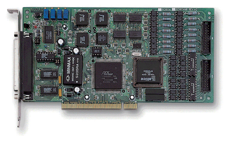
Comprehensive Product Summary: ADLINK PCI-9114HG Multi-Function Data Acquisition Card
### 1. Product Overview
Product Name: PCI-9114HG
Model: PCI-9114HG
Series: PCI-9114 Series – 32-Channel, 16-Bit, High-Resolution Multi-Function DAQ Cards
Article Number: PCI-9114HG
Manufacturer: ADLINK Technology Inc.
Product Type: PCI Bus Analog-to-Digital (A/D) Thermocouple and Multi-Function Data Acquisition Card
Category: PCI DAQ / Thermocouple Measurement Interface
The ADLINK PCI-9114HG is a high-gain, 16-bit, 32-channel analog input data acquisition card designed for precision thermocouple and transducer measurement applications. It integrates analog input, isolated digital I/O, and timing functions into a single PCI-bus plug-and-play card, offering high accuracy, isolation, and flexible software support for industrial and laboratory data acquisition systems.
### 2. Key Features
- High-Resolution Analog Input: 16-bit A/D conversion with up to 100 kS/s sampling rate.
- Channel Configuration: 32 single-ended or 16 differential analog input channels.
- Programmable Gain Amplifier (PGA): Software-selectable gains of 1, 10, 100, and 1000 for high-gain (HG) version.
- Input Range: Bipolar ±10 V, ±1 V, ±100 mV, ±10 mV (HG version).
- Cold Junction Compensation (CJC): On-board sensor for thermocouple measurement accuracy.
- Isolation: 16 isolated digital inputs and 16 isolated digital outputs, each with 2500–5000 V RMS isolation.
- Digital I/O:
- 16 isolated digital inputs (0–24 V, non-polarity).
- 16 isolated digital outputs (open-emitter Darlington transistor drivers, 5–35 V supply).
- Timer/Counter: One 16-bit general-purpose timer/counter (8254 compatible) with 2 MHz base clock.
- FIFO Buffer: 1K-sample hardware FIFO for analog input buffering.
- Trigger Modes: Software, pacer timer, and external 5 V/TTL trigger.
- Plug-and-Play PCI Interface: Fully compliant with 32-bit PCI bus architecture.
- Software Support: Comprehensive driver suite for Windows and DOS, including LabVIEW®, HP VEE™, DASYLab™, and OPC server support.
- Applications: Industrial process control, thermocouple and RTD measurement, biomedical instrumentation, and power monitoring.
### 3. Technical Specifications
Analog Input (A/D):
- Channels: 32 single-ended or 16 differential
- Resolution: 16 bits
- Converter: Burr-Brown ADS7805 or equivalent (successive approximation type)
- Sampling Rate: 100 kS/s (PCI-9114HG)
- Conversion Time: 10 µs
- Input Ranges (software programmable): ±10 V, ±1 V, ±100 mV, ±10 mV
- Input Coupling: DC
- Input Impedance: 1 GΩ (typical)
- Overvoltage Protection: Continuous ±35 V
- Trigger Modes: Software, pacer, external (TTL 5 V)
- FIFO Buffer: 1 K-sample (1024 words)
- Data Transfer: Polling, interrupt, or FIFO half-full interrupt
- Accuracy: ±0.01% of FSR ±1 LSB (typical)
Isolated Digital Input (IDI):
- Channels: 16
- Input Voltage Range: 0–24 VDC (non-polarity)
- Logic Levels:
- Logic Low: 0–1.5 V
- Logic High: 5–24 V
- Input Resistance: 2.4 kΩ @ 0.5 W
- Isolation Voltage: 2500–5000 V RMS
- Data Transfer: Programmed I/O
Isolated Digital Output (IDO):
- Channels: 16
- Output Type: Open-emitter Darlington transistor
- Supply Voltage: 5–35 VDC
- Sink Current:
- 350 mA per channel @ 100% duty
- 260 mA per channel @ 10% duty (all channels active)
- Power Dissipation: Max. 1.47 W per chip (8 DO channels)
- Isolation Voltage: 2500–5000 V RMS
Timer/Counter:
- Channels: 1 (8254 compatible)
- Resolution: 16 bits
- Base Clock: 2 MHz internal, external up to 2 MHz
- Modes: 6 programmable modes (rate generator, one-shot, etc.)
Power Output:
- +12 V and -12 V outputs with resettable 500 mA fuse protection
Physical & Environmental:
- Dimensions: 175 mm (L) × 107 mm (W)
- Weight: Approx. 200 g
- Operating Temperature: 0°C to 55°C
- Storage Temperature: -20°C to 80°C
- Humidity: 5–95% RH, non-condensing
- Power Requirements:
- +5 V @ 600 mA (typical)
- +12 V @ 100 mA (typical)
Connectors:
- CN1: 37-pin D-sub female (analog input)
- CN2: 20-pin ribbon male (isolated digital input)
- CN3: 20-pin ribbon male (isolated digital output)
### 4. Functionality
The PCI-9114HG operates as a high-precision data acquisition interface for analog and digital signals. It converts analog voltages into 16-bit digital data using a high-speed successive approximation A/D converter. The programmable gain amplifier allows flexible scaling of input signals for optimal resolution.
Use Cases:
- Thermocouple and RTD temperature measurement with cold junction compensation.
- Industrial process monitoring and control.
- Biomedical and physiological signal acquisition.
- Power system monitoring and transient analysis.
- General-purpose laboratory data logging.
Compatibility:
- Fully PCI 2.1 compliant, plug-and-play installation.
- Supported by ADLINK’s PCIS-DASK driver library for Windows 95/98/NT/2000 and DOS.
- Compatible with LabVIEW®, HP VEE™, DASYLab™, InTouch™, InControl™, ISaGRAF™, and OPC clients.
### 5. Components & Accessories
Included Items:
- PCI-9114HG DAQ Card
- ADLINK Software CD (drivers, utilities, manuals)
- Software Installation Guide
Optional Termination Boards:
- DIN-37D: 37-pin D-sub termination board with DIN-rail mounting (includes 1 m ACL-10137 cable).
- DIN-20P: 20-pin ribbon termination board with DIN-rail mounting (includes 1 m ACL-10120 cable).
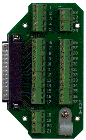
- ACLD-9137: General-purpose termination board with 37-pin D-sub male connector.
- ACLD-9188: Termination board with two 20-pin ribbon connectors and one 37-pin D-sub connector (includes two 1 m ACL-10120 cables).
### 6. Installation & Setup
Requirements:
- Available 32-bit PCI slot on host PC.
- Compatible operating system (Windows 95/98/NT/2000 or DOS).
Installation Steps:
1. Power off the computer and disconnect peripherals.
2. Insert the PCI-9114HG into an available PCI slot.
3. Secure the card and reconnect system power.
4. Upon boot, Windows Plug-and-Play will detect the card.
5. Install drivers from the ADLINK CD following the Software Installation Guide.
Jumper Configuration:
- JP1: Selects analog input type (Single-Ended or Differential).
- JP2: Enables or disables Cold Junction Sensor (CJC) connection.
Connector Pinouts:
- CN1: Analog input channels (AI0–AI31), AGND, ±12 V outputs.
- CN2: Isolated digital inputs (DI0–DI15) with EICOM1–EICOM4 commons.
- CN3: Isolated digital outputs (DO0–DO15) with EOGND and Vpower.
### 7. Performance & Capabilities
- Sampling Rate: 100 kS/s (single channel).
- Resolution: 16 bits (1 part in 65,536).
- Gain Accuracy: ±0.01% of full-scale range ±1 LSB.
- Noise Rejection: Differential mode for maximum noise immunity.
- FIFO Buffer: 1K-sample hardware buffer for continuous acquisition.
- Triggering: Software, pacer timer, or external TTL trigger.
- Data Transfer Modes:
- Polling (software-controlled)
- FIFO half-full polling
- End-of-conversion interrupt
- FIFO half-full interrupt
Limitations:
- Maximum throughput limited to 100 kS/s per channel.
- Analog input limited to ±35 V continuous overvoltage protection.
- Single PCI slot occupancy; no DMA transfer support.
### 8. Standards & Compliance
- Bus Interface: PCI Local Bus Specification Rev. 2.1 compliant.
- Isolation: 2500–5000 V RMS isolation for digital I/O.
- Safety & EMC: Designed for industrial environments with high noise immunity.
- Software Standards:
- OPC (OLE for Process Control) compliant server support.
- Compatible with IEC1131-3 SoftPLC environments (ISaGRAF™).
- Environmental Compliance: RoHS and CE compliant (depending on production batch).
### 9. Additional Information
Calibration & Maintenance:
- On-board variable resistors (VR1–VR4) for A/D offset, full-scale, PGA offset, and CJC calibration.
- Recommended recalibration interval:
- Every 3 months in industrial environments.
- Every 6–12 months in laboratory conditions.
- Software-based offset calibration supported for temperature drift compensation.
Utilities & Software Tools:
- 9114util.exe: System configuration, calibration, and functional testing utility.
- I_EEPROM.exe: Enables/disables interrupt functionality for compatibility management.
- PCIS-DASK Library: Comprehensive API for C/C++, VB, and Delphi.
- LabVIEW® VIs and HP VEE™ Objects: Included for graphical programming environments.
Warranty:
- One-year limited warranty against defects in materials and workmanship.
- Excludes damage from misuse, modification, or operation beyond specifications.
- Return-to-factory service; customer responsible for shipping and insurance.
Technical Support:
- ADLINK Technology Inc.
- Address: 9F, No. 166, Jian Yi Road, Chungho City, Taipei 235, Taiwan, R.O.C.
- Tel: +886-2-82265877
- Fax: +886-2-82265717
- Web: [www.adlinktech.com](http://www.adlinktech.com)
- Email: service@adlink.com.tw | nudaq@adlink.com.tw
Software Updates:
- Driver and utility updates available via ADLINK’s website.
- Backward compatibility maintained across Windows 95/98/NT/2000 platforms.
### Summary
The ADLINK PCI-9114HG is a robust, high-precision, multi-function data acquisition card engineered for demanding industrial and scientific applications. With 16-bit resolution, 32 analog input channels, programmable gain, and isolated digital I/O, it provides a complete solution for analog signal measurement, thermocouple interfacing, and process control. Its flexible software ecosystem, high isolation, and reliable PCI plug-and-play architecture make it a preferred choice for engineers and researchers requiring accurate, high-speed data acquisition in PC-based systems.

### 1. Product Overview
Product Name: PCI-9114HG
Model: PCI-9114HG
Series: PCI-9114 Series – 32-Channel, 16-Bit, High-Resolution Multi-Function DAQ Cards
Article Number: PCI-9114HG
Manufacturer: ADLINK Technology Inc.
Product Type: PCI Bus Analog-to-Digital (A/D) Thermocouple and Multi-Function Data Acquisition Card
Category: PCI DAQ / Thermocouple Measurement Interface
The ADLINK PCI-9114HG is a high-gain, 16-bit, 32-channel analog input data acquisition card designed for precision thermocouple and transducer measurement applications. It integrates analog input, isolated digital I/O, and timing functions into a single PCI-bus plug-and-play card, offering high accuracy, isolation, and flexible software support for industrial and laboratory data acquisition systems.
### 2. Key Features
- High-Resolution Analog Input: 16-bit A/D conversion with up to 100 kS/s sampling rate.
- Channel Configuration: 32 single-ended or 16 differential analog input channels.
- Programmable Gain Amplifier (PGA): Software-selectable gains of 1, 10, 100, and 1000 for high-gain (HG) version.
- Input Range: Bipolar ±10 V, ±1 V, ±100 mV, ±10 mV (HG version).
- Cold Junction Compensation (CJC): On-board sensor for thermocouple measurement accuracy.
- Isolation: 16 isolated digital inputs and 16 isolated digital outputs, each with 2500–5000 V RMS isolation.
- Digital I/O:
- 16 isolated digital inputs (0–24 V, non-polarity).
- 16 isolated digital outputs (open-emitter Darlington transistor drivers, 5–35 V supply).
- Timer/Counter: One 16-bit general-purpose timer/counter (8254 compatible) with 2 MHz base clock.
- FIFO Buffer: 1K-sample hardware FIFO for analog input buffering.
- Trigger Modes: Software, pacer timer, and external 5 V/TTL trigger.
- Plug-and-Play PCI Interface: Fully compliant with 32-bit PCI bus architecture.
- Software Support: Comprehensive driver suite for Windows and DOS, including LabVIEW®, HP VEE™, DASYLab™, and OPC server support.
- Applications: Industrial process control, thermocouple and RTD measurement, biomedical instrumentation, and power monitoring.
### 3. Technical Specifications
Analog Input (A/D):
- Channels: 32 single-ended or 16 differential
- Resolution: 16 bits
- Converter: Burr-Brown ADS7805 or equivalent (successive approximation type)
- Sampling Rate: 100 kS/s (PCI-9114HG)
- Conversion Time: 10 µs
- Input Ranges (software programmable): ±10 V, ±1 V, ±100 mV, ±10 mV
- Input Coupling: DC
- Input Impedance: 1 GΩ (typical)
- Overvoltage Protection: Continuous ±35 V
- Trigger Modes: Software, pacer, external (TTL 5 V)
- FIFO Buffer: 1 K-sample (1024 words)
- Data Transfer: Polling, interrupt, or FIFO half-full interrupt
- Accuracy: ±0.01% of FSR ±1 LSB (typical)
Isolated Digital Input (IDI):
- Channels: 16
- Input Voltage Range: 0–24 VDC (non-polarity)
- Logic Levels:
- Logic Low: 0–1.5 V
- Logic High: 5–24 V
- Input Resistance: 2.4 kΩ @ 0.5 W
- Isolation Voltage: 2500–5000 V RMS
- Data Transfer: Programmed I/O
Isolated Digital Output (IDO):
- Channels: 16
- Output Type: Open-emitter Darlington transistor
- Supply Voltage: 5–35 VDC
- Sink Current:
- 350 mA per channel @ 100% duty
- 260 mA per channel @ 10% duty (all channels active)
- Power Dissipation: Max. 1.47 W per chip (8 DO channels)
- Isolation Voltage: 2500–5000 V RMS
Timer/Counter:
- Channels: 1 (8254 compatible)
- Resolution: 16 bits
- Base Clock: 2 MHz internal, external up to 2 MHz
- Modes: 6 programmable modes (rate generator, one-shot, etc.)
Power Output:
- +12 V and -12 V outputs with resettable 500 mA fuse protection
Physical & Environmental:
- Dimensions: 175 mm (L) × 107 mm (W)
- Weight: Approx. 200 g
- Operating Temperature: 0°C to 55°C
- Storage Temperature: -20°C to 80°C
- Humidity: 5–95% RH, non-condensing
- Power Requirements:
- +5 V @ 600 mA (typical)
- +12 V @ 100 mA (typical)
Connectors:
- CN1: 37-pin D-sub female (analog input)
- CN2: 20-pin ribbon male (isolated digital input)
- CN3: 20-pin ribbon male (isolated digital output)
### 4. Functionality
The PCI-9114HG operates as a high-precision data acquisition interface for analog and digital signals. It converts analog voltages into 16-bit digital data using a high-speed successive approximation A/D converter. The programmable gain amplifier allows flexible scaling of input signals for optimal resolution.
Use Cases:
- Thermocouple and RTD temperature measurement with cold junction compensation.
- Industrial process monitoring and control.
- Biomedical and physiological signal acquisition.
- Power system monitoring and transient analysis.
- General-purpose laboratory data logging.
Compatibility:
- Fully PCI 2.1 compliant, plug-and-play installation.
- Supported by ADLINK’s PCIS-DASK driver library for Windows 95/98/NT/2000 and DOS.
- Compatible with LabVIEW®, HP VEE™, DASYLab™, InTouch™, InControl™, ISaGRAF™, and OPC clients.
### 5. Components & Accessories
Included Items:
- PCI-9114HG DAQ Card
- ADLINK Software CD (drivers, utilities, manuals)
- Software Installation Guide
Optional Termination Boards:
- DIN-37D: 37-pin D-sub termination board with DIN-rail mounting (includes 1 m ACL-10137 cable).
- DIN-20P: 20-pin ribbon termination board with DIN-rail mounting (includes 1 m ACL-10120 cable).
- ACLD-9137: General-purpose termination board with 37-pin D-sub male connector.
- ACLD-9188: Termination board with two 20-pin ribbon connectors and one 37-pin D-sub connector (includes two 1 m ACL-10120 cables).
### 6. Installation & Setup
Requirements:
- Available 32-bit PCI slot on host PC.
- Compatible operating system (Windows 95/98/NT/2000 or DOS).
Installation Steps:
1. Power off the computer and disconnect peripherals.
2. Insert the PCI-9114HG into an available PCI slot.
3. Secure the card and reconnect system power.
4. Upon boot, Windows Plug-and-Play will detect the card.
5. Install drivers from the ADLINK CD following the Software Installation Guide.
Jumper Configuration:
- JP1: Selects analog input type (Single-Ended or Differential).
- JP2: Enables or disables Cold Junction Sensor (CJC) connection.
Connector Pinouts:
- CN1: Analog input channels (AI0–AI31), AGND, ±12 V outputs.
- CN2: Isolated digital inputs (DI0–DI15) with EICOM1–EICOM4 commons.
- CN3: Isolated digital outputs (DO0–DO15) with EOGND and Vpower.
### 7. Performance & Capabilities
- Sampling Rate: 100 kS/s (single channel).
- Resolution: 16 bits (1 part in 65,536).
- Gain Accuracy: ±0.01% of full-scale range ±1 LSB.
- Noise Rejection: Differential mode for maximum noise immunity.
- FIFO Buffer: 1K-sample hardware buffer for continuous acquisition.
- Triggering: Software, pacer timer, or external TTL trigger.
- Data Transfer Modes:
- Polling (software-controlled)
- FIFO half-full polling
- End-of-conversion interrupt
- FIFO half-full interrupt
Limitations:
- Maximum throughput limited to 100 kS/s per channel.
- Analog input limited to ±35 V continuous overvoltage protection.
- Single PCI slot occupancy; no DMA transfer support.
### 8. Standards & Compliance
- Bus Interface: PCI Local Bus Specification Rev. 2.1 compliant.
- Isolation: 2500–5000 V RMS isolation for digital I/O.
- Safety & EMC: Designed for industrial environments with high noise immunity.
- Software Standards:
- OPC (OLE for Process Control) compliant server support.
- Compatible with IEC1131-3 SoftPLC environments (ISaGRAF™).
- Environmental Compliance: RoHS and CE compliant (depending on production batch).
### 9. Additional Information
Calibration & Maintenance:
- On-board variable resistors (VR1–VR4) for A/D offset, full-scale, PGA offset, and CJC calibration.
- Recommended recalibration interval:
- Every 3 months in industrial environments.
- Every 6–12 months in laboratory conditions.
- Software-based offset calibration supported for temperature drift compensation.
Utilities & Software Tools:
- 9114util.exe: System configuration, calibration, and functional testing utility.
- I_EEPROM.exe: Enables/disables interrupt functionality for compatibility management.
- PCIS-DASK Library: Comprehensive API for C/C++, VB, and Delphi.
- LabVIEW® VIs and HP VEE™ Objects: Included for graphical programming environments.
Warranty:
- One-year limited warranty against defects in materials and workmanship.
- Excludes damage from misuse, modification, or operation beyond specifications.
- Return-to-factory service; customer responsible for shipping and insurance.
Technical Support:
- ADLINK Technology Inc.
- Address: 9F, No. 166, Jian Yi Road, Chungho City, Taipei 235, Taiwan, R.O.C.
- Tel: +886-2-82265877
- Fax: +886-2-82265717
- Web: [www.adlinktech.com](http://www.adlinktech.com)
- Email: service@adlink.com.tw | nudaq@adlink.com.tw
Software Updates:
- Driver and utility updates available via ADLINK’s website.
- Backward compatibility maintained across Windows 95/98/NT/2000 platforms.
### Summary
The ADLINK PCI-9114HG is a robust, high-precision, multi-function data acquisition card engineered for demanding industrial and scientific applications. With 16-bit resolution, 32 analog input channels, programmable gain, and isolated digital I/O, it provides a complete solution for analog signal measurement, thermocouple interfacing, and process control. Its flexible software ecosystem, high isolation, and reliable PCI plug-and-play architecture make it a preferred choice for engineers and researchers requiring accurate, high-speed data acquisition in PC-based systems.
-
05-19.pdf
PDF Catalog
-
P9114 Manual.PDF
Manual
- ACLD-9188 - Panel for mounting low pass filter etc.
- ACLD-9137-01 - Direct 37 small screw terminal
- DIN-37D-01 - 37pin D-type panel DIN rail w/o cable
- ACL-10337 - 2*20 pin to DB 37 slot adapter