ACLD-9137-01
SUCHEN SIE DIE PASSENDE
INDUSTRIELLE LÖSUNG?
Entdecken Sie Embedded-, Kommunikations- und Automatisierungslösungen für Ihre Anwendung.
- Six Analog Output Channels:
Each channel features a 12‑bit resolution D/A converter (DAC7541AJP or equivalent) with double‑buffered architecture for smooth, single‑step updates.
- Multiple Output Ranges:
Configurable per channel for unipolar (0–5 V, 0–10 V), bipolar (±5 V, ±10 V), or current loop (4–20 mA sink) operation.
- Fast Conversion Performance:
Maximum settling time of 70 µs ensures rapid analog output updates suitable for dynamic control systems.
- Digital I/O Capability:
16 digital input and 16 digital output channels, all TTL/DTL compatible, supporting standard 74/74LS logic levels.
- Enhanced Interrupt Support:
Selectable IRQ levels (IRQ3–IRQ15) triggered by external digital input (pin 17 of CN3).
- Compatibility:
Register structure fully compatible with Advantech PCL‑726, simplifying software migration.
- Robust Design:
Surface‑mount technology (SMT) construction for improved reliability and reduced noise susceptibility.
- Compact Form Factor:
Half‑size ISA card (163 mm × 123 mm) suitable for standard PC/AT chassis.
- Software Support:
Includes DOS programming library (ACLS‑DLL2) and LabVIEW driver (ACLS‑LVIEW) for Windows 95/98/NT environments.
- Automatic Safe State:
All D/A outputs reset to 0 V upon power‑on or system reset.
Each channel features a 12‑bit resolution D/A converter (DAC7541AJP or equivalent) with double‑buffered architecture for smooth, single‑step updates.
- Multiple Output Ranges:
Configurable per channel for unipolar (0–5 V, 0–10 V), bipolar (±5 V, ±10 V), or current loop (4–20 mA sink) operation.
- Fast Conversion Performance:
Maximum settling time of 70 µs ensures rapid analog output updates suitable for dynamic control systems.
- Digital I/O Capability:
16 digital input and 16 digital output channels, all TTL/DTL compatible, supporting standard 74/74LS logic levels.
- Enhanced Interrupt Support:
Selectable IRQ levels (IRQ3–IRQ15) triggered by external digital input (pin 17 of CN3).
- Compatibility:
Register structure fully compatible with Advantech PCL‑726, simplifying software migration.
- Robust Design:
Surface‑mount technology (SMT) construction for improved reliability and reduced noise susceptibility.
- Compact Form Factor:
Half‑size ISA card (163 mm × 123 mm) suitable for standard PC/AT chassis.
- Software Support:
Includes DOS programming library (ACLS‑DLL2) and LabVIEW driver (ACLS‑LVIEW) for Windows 95/98/NT environments.
- Automatic Safe State:
All D/A outputs reset to 0 V upon power‑on or system reset.
Comprehensive Product Summary – ADLINK ACL‑6126 6‑Channel D/A Output & DIO Card
### 1. Product Overview
Product Name: ACL‑6126
Model Number: ACL‑6126
Series: NuDAQ ISA‑Bus Analog Output & Digital I/O Series
Article Number: ACL‑6126
Manufacturer: ADLINK Technology Inc.
Manufacturer Address: 9F, No. 166, Jian Yi Road, Chungho City, Taipei 235, Taiwan, R.O.C.
Website: [www.adlink.com.tw](http://www.adlink.com.tw)
Support Contacts:
- General Service: service@adlink.com.tw
- Technical Support (NuDAQ): nudaq@adlink.com.tw
- Software Support: sw@adlink.com.tw
- Telephone: +886‑2‑82265877
- Fax: +886‑2‑82265717
Product Description:
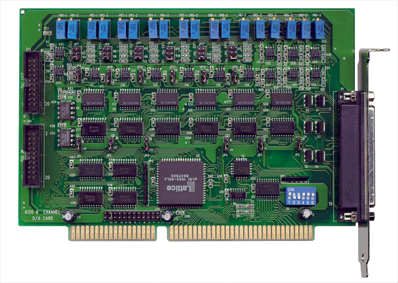
The ADLINK ACL‑6126 is a 6‑channel analog output and 32‑channel digital I/O expansion card designed for PC/AT‑compatible systems. It provides six 12‑bit D/A output channels with multiple selectable voltage and current ranges, along with 16 TTL‑compatible digital inputs and 16 TTL‑compatible digital outputs. The card is optimized for industrial control, laboratory automation, and programmable signal generation applications requiring precise analog output and digital control capabilities.
### 2. Key Features
- Six Analog Output Channels:
Each channel features a 12‑bit resolution D/A converter (DAC7541AJP or equivalent) with double‑buffered architecture for smooth, single‑step updates.
- Multiple Output Ranges:
Configurable per channel for unipolar (0–5 V, 0–10 V), bipolar (±5 V, ±10 V), or current loop (4–20 mA sink) operation.
- Fast Conversion Performance:
Maximum settling time of 70 µs ensures rapid analog output updates suitable for dynamic control systems.
- Digital I/O Capability:
16 digital input and 16 digital output channels, all TTL/DTL compatible, supporting standard 74/74LS logic levels.
- Enhanced Interrupt Support:
Selectable IRQ levels (IRQ3–IRQ15) triggered by external digital input (pin 17 of CN3).
- Compatibility:
Register structure fully compatible with Advantech PCL‑726, simplifying software migration.
- Robust Design:
Surface‑mount technology (SMT) construction for improved reliability and reduced noise susceptibility.
- Compact Form Factor:
Half‑size ISA card (163 mm × 123 mm) suitable for standard PC/AT chassis.
- Software Support:
Includes DOS programming library (ACLS‑DLL2) and LabVIEW driver (ACLS‑LVIEW) for Windows 95/98/NT environments.
- Automatic Safe State:
All D/A outputs reset to 0 V upon power‑on or system reset.
### 3. Technical Specifications
Analog Output (D/A):
- Converter Type: DAC7541AJP or equivalent, monolithic multiplying DAC
- Channels: 6 independent analog outputs
- Resolution: 12 bits, double‑buffered
- Output Ranges:
- Unipolar: 0 – +5 V or 0 – +10 V
- Bipolar: ±5 V or ±10 V
- Current Loop: 4 – 20 mA (sink mode)
- Reference Voltage:
- Internal: −5 V or −10 V
- External: ±10 V (DC or AC reference input via REF.IN)
- Settling Time: ≤ 70 µs
- Linearity Error: ±½ LSB
- Accuracy: ±0.012 % of full‑scale range
- Voltage Drive Capability: ±5 mA maximum
- Current Loop Excitation Voltage: 8 V (min) – 36 V (max)
- Output Initial State: 0 V after reset or power‑on
Digital Input (D/I):
- Channels: 16
- Logic Level: TTL compatible
- Input Low Voltage: −0.5 V (min), 0.8 V (max)
- Input High Voltage: 2.0 V (min), 5.0 V (max)
- Input Current: ≤ 0.2 mA at 0.4 V
- Input Hysteresis: 0.2 V (min), 0.4 V (typical)
Digital Output (D/O):
- Channels: 16
- Logic Level: TTL compatible
- Output Low Voltage (Sink): ≤ 0.5 V @ 24 mA, ≤ 0.4 V @ 12 mA
- Output High Voltage (Source): ≥ 2.0 V @ 15 mA, ≥ 2.4 V @ 3 mA
- Drive Capability: Supports standard TTL (74 series) and LSTTL (74LS) loads
General:
- Bus Interface: PC/AT ISA bus
- Connectors:
- CN3: 37‑pin D‑sub (analog outputs and reference input)
- CN1: 20‑pin IDC (digital outputs)
- CN2: 20‑pin IDC (digital inputs)
- Operating Temperature: 0 °C – 55 °C
- Storage Temperature: −20 °C – 80 °C
- Relative Humidity: 5 % – 95 %, non‑condensing
- Power Requirements:
- +5 V @ 360 mA (typ), 450 mA (max)
- +12 V @ 60 mA (typ), 180 mA (max)
- −12 V @ 20 mA (typ), 90 mA (max)
- Dimensions: 163 mm (L) × 123 mm (W) (half‑size ISA card)
### 4. Functionality
The ACL‑6126 operates as an analog and digital I/O expansion card for PC/AT‑compatible systems. It converts digital data from the host computer into precise analog voltage or current outputs through six independent D/A channels. Each channel can be configured for unipolar, bipolar, or current‑sink operation using onboard jumpers.
Operation Principle:
- Digital data written to the card’s I/O registers (Base + 0 – Base + 11) are converted to analog signals by the DACs.
- Each D/A channel has a double buffer, allowing new data to be preloaded and updated simultaneously for synchronized output.
- Digital I/O channels are accessed via Base + 12 – Base + 15 registers, enabling bit‑level control and monitoring.
Use Cases and Applications:
- Industrial process control and automation
- Laboratory instrumentation and test systems
- Programmable voltage or current sources
- Function and waveform generation
- Energy management and building automation
- Security and access control systems
- Programmable current sink or loop control applications
Compatibility:
- Fully compatible with Advantech PCL‑726 register structure
- Supported by ADLINK’s NuDAQ software suite and LabVIEW drivers
### 5. Components & Accessories
Included Items:
- ACL‑6126 6‑Channel Analog Output & DIO Card
- ADLINK Software CD (includes DOS library, Windows drivers, and sample programs)
- User’s Manual
Optional Accessories:
- ACLD‑9182: 16‑bit isolated digital input board
- ACLD‑9185: 16‑bit relay output board
- Shielded cables and terminal boards for CN1/CN2/CN3 connectors
Connectors:
- CN3 (37‑pin D‑sub): Analog outputs, reference voltage input, external trigger
- CN1 (20‑pin IDC): Digital outputs (DO0–DO15)
- CN2 (20‑pin IDC): Digital inputs (DI0–DI15)
External Trigger:
Pin 17 of CN3 provides an external interrupt trigger input for IRQ generation.
### 6. Installation & Setup
Pre‑Installation Handling:
- Handle the card on a grounded anti‑static mat using an ESD wrist strap.
- Inspect for physical damage before installation.
Installation Steps:
1. Power off the PC and remove the cover.
2. Insert the ACL‑6126 into an available ISA slot.
3. Secure the card with a screw to the chassis bracket.
4. Connect analog and digital cables to CN3, CN1, and CN2 as required.
5. Configure jumpers and DIP switches as needed (see below).
Configuration Options:
- Base Address: Selectable via 5‑position DIP switch (SW1). Default: 0x2C0.
- IRQ Level: Selectable via jumper JP7 (IRQ3–IRQ15). Default: IRQ15.
- Reference Voltage Source: Internal (−5 V or −10 V) or external (±10 V via REF.IN).
- Output Mode: Per‑channel jumper configuration for unipolar or bipolar operation.
- Current Loop Mode: Set to internal −5 V reference and unipolar mode; requires external 8–36 V supply.
Signal Connections:
- Voltage Output: Connect V.OUT and A.GND to the load or amplifier input.
- Current Sink Output: Connect I.OUT and A.GND to the load and external power supply (12 V or 24 V recommended).
Software Installation:
1. Insert ADLINK CD and navigate to `\NuDAQISA\6126`.
2. Run `SETUP` to install DOS utilities and libraries.
3. Files are installed to `C:\ADLINK\6126\DOS`.
4. Run `6126UTIL` for configuration and calibration.
5. Sample C programs are provided in the `\SAMPLES` directory.
### 7. Performance & Capabilities
- Analog Output Speed: Up to 15 kS/s per channel (typical operational rate).
- Settling Time: ≤ 70 µs to 0.012 % full‑scale accuracy.
- Resolution: 12 bits (4096 discrete levels).
- Output Drive: ±5 mA maximum per channel.
- Current Loop Range: 4–20 mA sink, 8–36 V compliance voltage.
- Digital I/O Throughput: TTL‑level switching suitable for high‑speed control.
- Interrupt Handling: Hardware interrupt via external trigger, selectable IRQ3–IRQ15.
- Limitations:
- ISA‑bus interface limits data throughput compared to modern PCI/PCIe cards.
- No onboard isolation; external isolation boards recommended for high‑voltage environments.
### 8. Standards & Compliance
- Bus Standard: PC/AT ISA bus (16‑bit)
- Electrical Interface: TTL/DTL compatible digital I/O
- Environmental Compliance:
- Operating temperature: 0 °C – 55 °C
- Storage temperature: −20 °C – 80 °C
- Humidity: 5 % – 95 %, non‑condensing
- Design Quality: SMT construction for enhanced reliability
- Compatibility: Register‑level compatibility with Advantech PCL‑726
- Safety & EMC: Designed for industrial PC environments (no explicit CE/FCC data provided in manual)
### 9. Additional Information
Warranty:
- One‑year limited warranty from date of purchase.
- Covers defects in materials and workmanship under normal use.
- Excludes damage from misuse, modification, or operation beyond specifications.
- Warranty service requires proof of purchase; return shipping prepaid.
Support & Maintenance:
- ADLINK provides technical support via email and phone.
- Software updates and drivers available through ADLINK’s website.
- Recommended periodic calibration for analog outputs using provided utilities.
Software & Development Tools:
- ACLS‑DLL2: Development kit for DOS/Windows 3.1/95/98/NT supporting C/C++, VB, Delphi.
- ACLS‑LVIEW: LabVIEW driver package for Windows 95/98/NT.
- Sample Programs: Demonstration utilities for analog output (DA_DEMO.C), digital input (DI_DEMO.C), and digital output (DO_DEMO.C).
Maintenance Recommendations:
- Keep connectors clean and free from dust.
- Avoid exposure to excessive humidity or vibration.
- Verify jumper settings after extended storage or transport.
Product Lifecycle Notes:
- Original manual revision 3.35 (June 1, 2000).
- Product subject to design improvements without prior notice.
### Summary
The ADLINK ACL‑6126 is a versatile, high‑precision 6‑channel analog output and 32‑channel digital I/O card for ISA‑bus PCs. It combines 12‑bit D/A conversion, flexible voltage/current output ranges, and robust TTL digital interfacing in a compact half‑size form factor. With fast 70 µs settling time, selectable IRQs, and comprehensive software support, it is ideal for industrial automation, laboratory instrumentation, and programmable signal generation tasks. The card’s modular jumper configuration allows per‑channel customization, while ADLINK’s software libraries and LabVIEW drivers simplify integration into both legacy and modern control systems.
Backed by ADLINK’s one‑year warranty and technical support, the ACL‑6126 remains a reliable solution for engineers requiring precise analog output and digital control in PC‑based measurement and automation environments.

### 1. Product Overview
Product Name: ACL‑6126
Model Number: ACL‑6126
Series: NuDAQ ISA‑Bus Analog Output & Digital I/O Series
Article Number: ACL‑6126
Manufacturer: ADLINK Technology Inc.
Manufacturer Address: 9F, No. 166, Jian Yi Road, Chungho City, Taipei 235, Taiwan, R.O.C.
Website: [www.adlink.com.tw](http://www.adlink.com.tw)
Support Contacts:
- General Service: service@adlink.com.tw
- Technical Support (NuDAQ): nudaq@adlink.com.tw
- Software Support: sw@adlink.com.tw
- Telephone: +886‑2‑82265877
- Fax: +886‑2‑82265717
Product Description:
The ADLINK ACL‑6126 is a 6‑channel analog output and 32‑channel digital I/O expansion card designed for PC/AT‑compatible systems. It provides six 12‑bit D/A output channels with multiple selectable voltage and current ranges, along with 16 TTL‑compatible digital inputs and 16 TTL‑compatible digital outputs. The card is optimized for industrial control, laboratory automation, and programmable signal generation applications requiring precise analog output and digital control capabilities.
### 2. Key Features
- Six Analog Output Channels:
Each channel features a 12‑bit resolution D/A converter (DAC7541AJP or equivalent) with double‑buffered architecture for smooth, single‑step updates.
- Multiple Output Ranges:
Configurable per channel for unipolar (0–5 V, 0–10 V), bipolar (±5 V, ±10 V), or current loop (4–20 mA sink) operation.
- Fast Conversion Performance:
Maximum settling time of 70 µs ensures rapid analog output updates suitable for dynamic control systems.
- Digital I/O Capability:
16 digital input and 16 digital output channels, all TTL/DTL compatible, supporting standard 74/74LS logic levels.
- Enhanced Interrupt Support:
Selectable IRQ levels (IRQ3–IRQ15) triggered by external digital input (pin 17 of CN3).
- Compatibility:
Register structure fully compatible with Advantech PCL‑726, simplifying software migration.
- Robust Design:
Surface‑mount technology (SMT) construction for improved reliability and reduced noise susceptibility.
- Compact Form Factor:
Half‑size ISA card (163 mm × 123 mm) suitable for standard PC/AT chassis.
- Software Support:
Includes DOS programming library (ACLS‑DLL2) and LabVIEW driver (ACLS‑LVIEW) for Windows 95/98/NT environments.
- Automatic Safe State:
All D/A outputs reset to 0 V upon power‑on or system reset.
### 3. Technical Specifications
Analog Output (D/A):
- Converter Type: DAC7541AJP or equivalent, monolithic multiplying DAC
- Channels: 6 independent analog outputs
- Resolution: 12 bits, double‑buffered
- Output Ranges:
- Unipolar: 0 – +5 V or 0 – +10 V
- Bipolar: ±5 V or ±10 V
- Current Loop: 4 – 20 mA (sink mode)
- Reference Voltage:
- Internal: −5 V or −10 V
- External: ±10 V (DC or AC reference input via REF.IN)
- Settling Time: ≤ 70 µs
- Linearity Error: ±½ LSB
- Accuracy: ±0.012 % of full‑scale range
- Voltage Drive Capability: ±5 mA maximum
- Current Loop Excitation Voltage: 8 V (min) – 36 V (max)
- Output Initial State: 0 V after reset or power‑on
Digital Input (D/I):
- Channels: 16
- Logic Level: TTL compatible
- Input Low Voltage: −0.5 V (min), 0.8 V (max)
- Input High Voltage: 2.0 V (min), 5.0 V (max)
- Input Current: ≤ 0.2 mA at 0.4 V
- Input Hysteresis: 0.2 V (min), 0.4 V (typical)
Digital Output (D/O):
- Channels: 16
- Logic Level: TTL compatible
- Output Low Voltage (Sink): ≤ 0.5 V @ 24 mA, ≤ 0.4 V @ 12 mA
- Output High Voltage (Source): ≥ 2.0 V @ 15 mA, ≥ 2.4 V @ 3 mA
- Drive Capability: Supports standard TTL (74 series) and LSTTL (74LS) loads
General:
- Bus Interface: PC/AT ISA bus
- Connectors:
- CN3: 37‑pin D‑sub (analog outputs and reference input)
- CN1: 20‑pin IDC (digital outputs)
- CN2: 20‑pin IDC (digital inputs)
- Operating Temperature: 0 °C – 55 °C
- Storage Temperature: −20 °C – 80 °C
- Relative Humidity: 5 % – 95 %, non‑condensing
- Power Requirements:
- +5 V @ 360 mA (typ), 450 mA (max)
- +12 V @ 60 mA (typ), 180 mA (max)
- −12 V @ 20 mA (typ), 90 mA (max)
- Dimensions: 163 mm (L) × 123 mm (W) (half‑size ISA card)
### 4. Functionality
The ACL‑6126 operates as an analog and digital I/O expansion card for PC/AT‑compatible systems. It converts digital data from the host computer into precise analog voltage or current outputs through six independent D/A channels. Each channel can be configured for unipolar, bipolar, or current‑sink operation using onboard jumpers.
Operation Principle:
- Digital data written to the card’s I/O registers (Base + 0 – Base + 11) are converted to analog signals by the DACs.
- Each D/A channel has a double buffer, allowing new data to be preloaded and updated simultaneously for synchronized output.
- Digital I/O channels are accessed via Base + 12 – Base + 15 registers, enabling bit‑level control and monitoring.
Use Cases and Applications:
- Industrial process control and automation
- Laboratory instrumentation and test systems
- Programmable voltage or current sources
- Function and waveform generation
- Energy management and building automation
- Security and access control systems
- Programmable current sink or loop control applications
Compatibility:
- Fully compatible with Advantech PCL‑726 register structure
- Supported by ADLINK’s NuDAQ software suite and LabVIEW drivers
### 5. Components & Accessories
Included Items:
- ACL‑6126 6‑Channel Analog Output & DIO Card
- ADLINK Software CD (includes DOS library, Windows drivers, and sample programs)
- User’s Manual
Optional Accessories:
- ACLD‑9182: 16‑bit isolated digital input board
- ACLD‑9185: 16‑bit relay output board
- Shielded cables and terminal boards for CN1/CN2/CN3 connectors
Connectors:
- CN3 (37‑pin D‑sub): Analog outputs, reference voltage input, external trigger
- CN1 (20‑pin IDC): Digital outputs (DO0–DO15)
- CN2 (20‑pin IDC): Digital inputs (DI0–DI15)
External Trigger:
Pin 17 of CN3 provides an external interrupt trigger input for IRQ generation.
### 6. Installation & Setup
Pre‑Installation Handling:
- Handle the card on a grounded anti‑static mat using an ESD wrist strap.
- Inspect for physical damage before installation.
Installation Steps:
1. Power off the PC and remove the cover.
2. Insert the ACL‑6126 into an available ISA slot.
3. Secure the card with a screw to the chassis bracket.
4. Connect analog and digital cables to CN3, CN1, and CN2 as required.
5. Configure jumpers and DIP switches as needed (see below).
Configuration Options:
- Base Address: Selectable via 5‑position DIP switch (SW1). Default: 0x2C0.
- IRQ Level: Selectable via jumper JP7 (IRQ3–IRQ15). Default: IRQ15.
- Reference Voltage Source: Internal (−5 V or −10 V) or external (±10 V via REF.IN).
- Output Mode: Per‑channel jumper configuration for unipolar or bipolar operation.
- Current Loop Mode: Set to internal −5 V reference and unipolar mode; requires external 8–36 V supply.
Signal Connections:
- Voltage Output: Connect V.OUT and A.GND to the load or amplifier input.
- Current Sink Output: Connect I.OUT and A.GND to the load and external power supply (12 V or 24 V recommended).
Software Installation:
1. Insert ADLINK CD and navigate to `\NuDAQISA\6126`.
2. Run `SETUP` to install DOS utilities and libraries.
3. Files are installed to `C:\ADLINK\6126\DOS`.
4. Run `6126UTIL` for configuration and calibration.
5. Sample C programs are provided in the `\SAMPLES` directory.
### 7. Performance & Capabilities
- Analog Output Speed: Up to 15 kS/s per channel (typical operational rate).
- Settling Time: ≤ 70 µs to 0.012 % full‑scale accuracy.
- Resolution: 12 bits (4096 discrete levels).
- Output Drive: ±5 mA maximum per channel.
- Current Loop Range: 4–20 mA sink, 8–36 V compliance voltage.
- Digital I/O Throughput: TTL‑level switching suitable for high‑speed control.
- Interrupt Handling: Hardware interrupt via external trigger, selectable IRQ3–IRQ15.
- Limitations:
- ISA‑bus interface limits data throughput compared to modern PCI/PCIe cards.
- No onboard isolation; external isolation boards recommended for high‑voltage environments.
### 8. Standards & Compliance
- Bus Standard: PC/AT ISA bus (16‑bit)
- Electrical Interface: TTL/DTL compatible digital I/O
- Environmental Compliance:
- Operating temperature: 0 °C – 55 °C
- Storage temperature: −20 °C – 80 °C
- Humidity: 5 % – 95 %, non‑condensing
- Design Quality: SMT construction for enhanced reliability
- Compatibility: Register‑level compatibility with Advantech PCL‑726
- Safety & EMC: Designed for industrial PC environments (no explicit CE/FCC data provided in manual)
### 9. Additional Information
Warranty:
- One‑year limited warranty from date of purchase.
- Covers defects in materials and workmanship under normal use.
- Excludes damage from misuse, modification, or operation beyond specifications.
- Warranty service requires proof of purchase; return shipping prepaid.
Support & Maintenance:
- ADLINK provides technical support via email and phone.
- Software updates and drivers available through ADLINK’s website.
- Recommended periodic calibration for analog outputs using provided utilities.
Software & Development Tools:
- ACLS‑DLL2: Development kit for DOS/Windows 3.1/95/98/NT supporting C/C++, VB, Delphi.
- ACLS‑LVIEW: LabVIEW driver package for Windows 95/98/NT.
- Sample Programs: Demonstration utilities for analog output (DA_DEMO.C), digital input (DI_DEMO.C), and digital output (DO_DEMO.C).
Maintenance Recommendations:
- Keep connectors clean and free from dust.
- Avoid exposure to excessive humidity or vibration.
- Verify jumper settings after extended storage or transport.
Product Lifecycle Notes:
- Original manual revision 3.35 (June 1, 2000).
- Product subject to design improvements without prior notice.
### Summary
The ADLINK ACL‑6126 is a versatile, high‑precision 6‑channel analog output and 32‑channel digital I/O card for ISA‑bus PCs. It combines 12‑bit D/A conversion, flexible voltage/current output ranges, and robust TTL digital interfacing in a compact half‑size form factor. With fast 70 µs settling time, selectable IRQs, and comprehensive software support, it is ideal for industrial automation, laboratory instrumentation, and programmable signal generation tasks. The card’s modular jumper configuration allows per‑channel customization, while ADLINK’s software libraries and LabVIEW drivers simplify integration into both legacy and modern control systems.
Backed by ADLINK’s one‑year warranty and technical support, the ACL‑6126 remains a reliable solution for engineers requiring precise analog output and digital control in PC‑based measurement and automation environments.
-
A6126 Manual.PDF
Manual
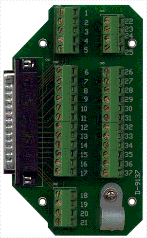
- ACLD-9137-01 - Direct 37 small screw terminal
- ACLD-9188 - Panel for mounting low pass filter etc.
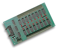
- ACLD-9185-01 - isolated 16 DO Relay panel
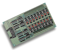
- ACLD-9182A-01 - isolated 16 DI (DC) panel
- DIN-37D-01 - 37pin D-type panel DIN rail w/o cable