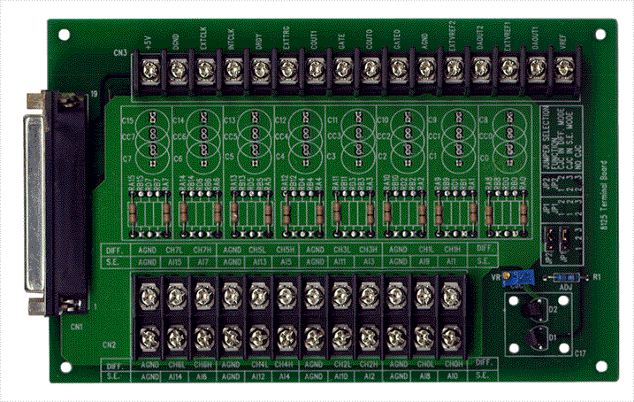
ACLD-8125
SUCHEN SIE DIE PASSENDE
INDUSTRIELLE LÖSUNG?
Entdecken Sie Embedded-, Kommunikations- und Automatisierungslösungen für Ihre Anwendung.
- Bus Interface: AT‑Bus (ISA)
- Analog Inputs: 16 single‑ended or 8 differential channels
- Analog Outputs: Two 12‑bit double‑buffered D/A channels
- Digital I/O: 16 digital inputs and 16 digital outputs (TTL/DTL compatible)
- Resolution: 12‑bit A/D and 12‑bit D/A
- Sampling Rate: Up to 100 kS/s (single channel)
- Programmable Gain:
- High‑gain programmable amplifier with 8 gain levels: ×0.5, ×1, ×5, ×10, ×50, ×100, ×500, ×1000
- Input Range (Programmable):
- Bipolar: ±10V, ±5V, ±1V, ±500mV, ±100mV, ±50mV, ±10mV, ±5mV
- Unipolar: 0–10V, 0–1V, 0–0.1V, 0–0.01V
- Trigger Modes: Software, internal pacer (timer), or external trigger
- Data Transfer Modes: Polling, DMA, or interrupt‑driven
- Timer/Counter:
- 8254 programmable interval timer with three 16‑bit counters
- Two cascaded counters for A/D pacer (32‑bit timer, 2 MHz base)
- One 16‑bit general‑purpose counter
- Interrupts: 9 selectable IRQ levels (IRQ3, 5–7, 9–12, 15)
- DMA Channels: Selectable CH1 or CH3
- Power Supply: On‑board DC/DC converter for stable analog power
- Connectors:
- 37‑pin D‑type female connector (analog I/O, counter/timer)
- Two 20‑pin IDC connectors (digital I/O)
- Form Factor: Half‑size ISA card (compact design)
- Software Support: C‑language library, DOS utilities, LabVIEW driver, and Windows SDK (ACLS‑DLL2)
- Analog Inputs: 16 single‑ended or 8 differential channels
- Analog Outputs: Two 12‑bit double‑buffered D/A channels
- Digital I/O: 16 digital inputs and 16 digital outputs (TTL/DTL compatible)
- Resolution: 12‑bit A/D and 12‑bit D/A
- Sampling Rate: Up to 100 kS/s (single channel)
- Programmable Gain:
- High‑gain programmable amplifier with 8 gain levels: ×0.5, ×1, ×5, ×10, ×50, ×100, ×500, ×1000
- Input Range (Programmable):
- Bipolar: ±10V, ±5V, ±1V, ±500mV, ±100mV, ±50mV, ±10mV, ±5mV
- Unipolar: 0–10V, 0–1V, 0–0.1V, 0–0.01V
- Trigger Modes: Software, internal pacer (timer), or external trigger
- Data Transfer Modes: Polling, DMA, or interrupt‑driven
- Timer/Counter:
- 8254 programmable interval timer with three 16‑bit counters
- Two cascaded counters for A/D pacer (32‑bit timer, 2 MHz base)
- One 16‑bit general‑purpose counter
- Interrupts: 9 selectable IRQ levels (IRQ3, 5–7, 9–12, 15)
- DMA Channels: Selectable CH1 or CH3
- Power Supply: On‑board DC/DC converter for stable analog power
- Connectors:
- 37‑pin D‑type female connector (analog I/O, counter/timer)
- Two 20‑pin IDC connectors (digital I/O)
- Form Factor: Half‑size ISA card (compact design)
- Software Support: C‑language library, DOS utilities, LabVIEW driver, and Windows SDK (ACLS‑DLL2)
Comprehensive Product Summary – ADLINK ACL‑8112HG High‑Gain Multifunction Data Acquisition Card
### 1. Product Overview
Product Name: ACL‑8112HG
Model: ACL‑8112HG
Series: ACL‑8112 Series (Enhanced Multi‑Function Data Acquisition Cards)
Article Number: ACL‑8112HG
Manufacturer: ADLINK Technology Inc.
Trademark: NuDAQ®
Product Description:
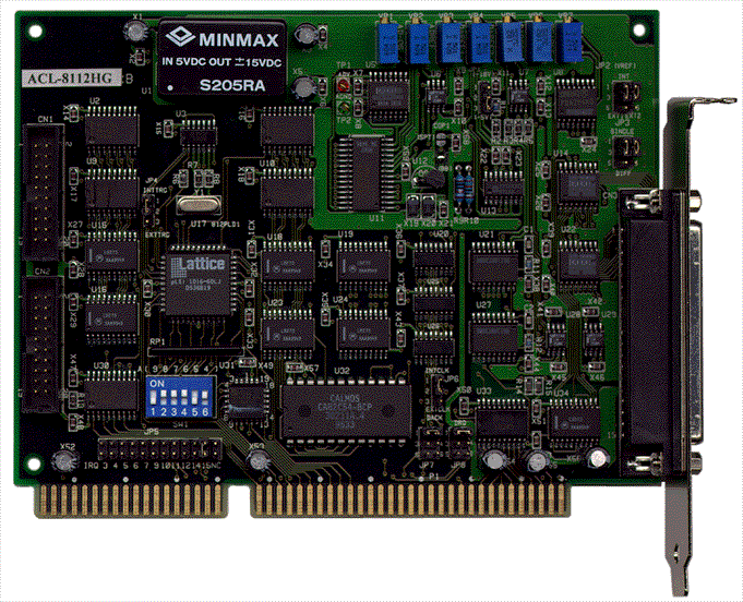
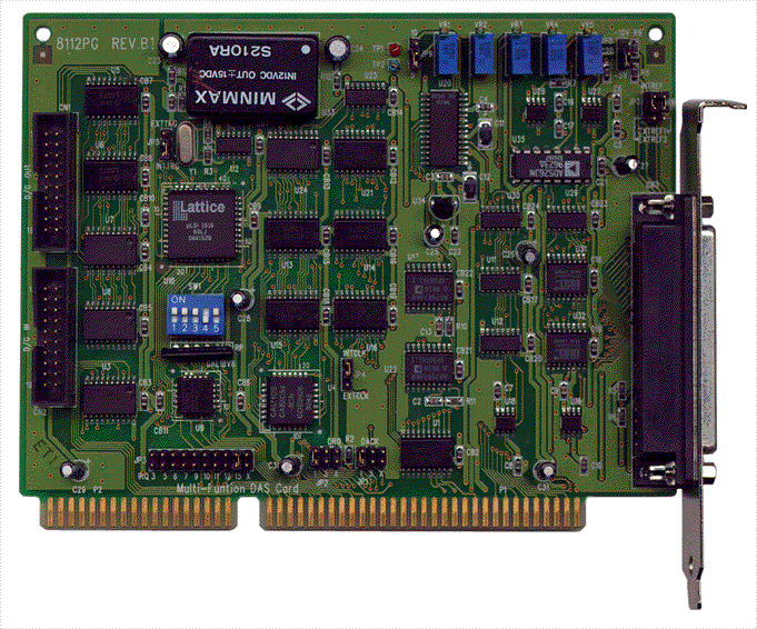
The ADLINK ACL‑8112HG is a high‑performance, high‑speed, multifunction data acquisition (DAQ) card designed for IBM PC/AT and compatible systems. It integrates analog‑to‑digital (A/D) conversion, digital‑to‑analog (D/A) conversion, digital input/output (DIO), and timer/counter functions on a single half‑size ISA card. The “HG” variant (High Gain) includes a programmable instrumentation amplifier for low‑level signal measurement, making it ideal for precision applications such as thermocouple and sensor data acquisition.
### 2. Key Features
- Bus Interface: AT‑Bus (ISA)
- Analog Inputs: 16 single‑ended or 8 differential channels
- Analog Outputs: Two 12‑bit double‑buffered D/A channels
- Digital I/O: 16 digital inputs and 16 digital outputs (TTL/DTL compatible)
- Resolution: 12‑bit A/D and 12‑bit D/A
- Sampling Rate: Up to 100 kS/s (single channel)
- Programmable Gain:
- High‑gain programmable amplifier with 8 gain levels: ×0.5, ×1, ×5, ×10, ×50, ×100, ×500, ×1000
- Input Range (Programmable):
- Bipolar: ±10V, ±5V, ±1V, ±500mV, ±100mV, ±50mV, ±10mV, ±5mV
- Unipolar: 0–10V, 0–1V, 0–0.1V, 0–0.01V
- Trigger Modes: Software, internal pacer (timer), or external trigger
- Data Transfer Modes: Polling, DMA, or interrupt‑driven
- Timer/Counter:
- 8254 programmable interval timer with three 16‑bit counters
- Two cascaded counters for A/D pacer (32‑bit timer, 2 MHz base)
- One 16‑bit general‑purpose counter
- Interrupts: 9 selectable IRQ levels (IRQ3, 5–7, 9–12, 15)
- DMA Channels: Selectable CH1 or CH3
- Power Supply: On‑board DC/DC converter for stable analog power
- Connectors:
- 37‑pin D‑type female connector (analog I/O, counter/timer)
- Two 20‑pin IDC connectors (digital I/O)
- Form Factor: Half‑size ISA card (compact design)
- Software Support: C‑language library, DOS utilities, LabVIEW driver, and Windows SDK (ACLS‑DLL2)
### 3. Technical Specifications
Analog Input (A/D):
- Converter Type: ADS774 or equivalent, successive approximation
- Resolution: 12 bits
- Channels: 16 SE or 8 DIFF
- Input Impedance: 10 MΩ
- Conversion Time: 8 µs
- Overvoltage Protection: ±35V continuous
- Accuracy (ACL‑8112HG):
- Gain ×0.5, ×1: ±0.01% FSR ±1 LSB
- Gain ×5, ×10: ±0.02% FSR ±1 LSB
- Gain ×50, ×100: ±0.04% FSR ±1 LSB
- Gain ×500, ×1000: ±0.04% FSR ±1 LSB
- Sampling Rate:
- 100 kHz max (single channel)
- 20 kHz max (multiplexed)
- Trigger Modes: Software, pacer, external
- Data Transfer: Polling, DMA, interrupt
Analog Output (D/A):
- Converter: DAC7541 or equivalent
- Channels: 2 (double‑buffered)
- Resolution: 12 bits
- Output Range:
- Internal reference: 0–5V or 0–10V (unipolar)
- External reference: ±10V max
- Settling Time: 30 µs
- Linearity: ±½ LSB
- Output Drive: ±5 mA max
Digital I/O:
- Channels: 16 inputs, 16 outputs (TTL compatible)
- Input Voltage:
- Low ≤ 0.8V, High ≥ 2.0V
- Output Voltage:
- Low ≤ 0.4V @ 8 mA sink
- High ≥ 2.4V @ 0.4 mA source
Timer/Counter:
- Device: Intel/NEC 8254
- Counters: 3 × 16‑bit
- A/D Pacer: Two cascaded counters (32‑bit)
- Base Clock: 2 MHz
- Output Frequency: 0.00046 Hz – 100 kHz
- Counter 0: User‑programmable (event counting, frequency generation)
General:
- I/O Base Address: 16 consecutive locations (default 0x220)
- IRQ Levels: 3, 5–7, 9–12, 15
- DMA Channels: 1 or 3 (jumper‑selectable)
- Operating Temperature: 0–55 °C
- Storage Temperature: –20–80 °C
- Humidity: 5–95% non‑condensing
- Power Consumption:
- +5 V @ 430 mA typical
- +12 V @ 150 mA typical
- Dimensions: 162 mm (L) × 115 mm (W)
- Weight: Approx. 200 g (typical board weight)
### 4. Functionality
Operation Principle:
The ACL‑8112HG performs high‑speed data acquisition by converting analog signals into 12‑bit digital values using a successive‑approximation A/D converter. The programmable gain amplifier allows precise scaling of low‑level signals. The card supports both unipolar and bipolar input ranges, selectable via software or jumpers.
Use Cases & Applications:
- Industrial process monitoring and control
- Laboratory instrumentation and test automation
- Thermocouple and sensor signal acquisition
- Energy management and environmental monitoring
- Event counting, pulse width, and frequency measurement
- Waveform generation and control signal output
- Security and annunciation systems
Compatibility:
- IBM PC/AT and compatible ISA‑bus systems
- Supported operating systems: DOS, Windows 3.1/95/98/NT (via SDK)
- Software environments: C/C++, Visual Basic, Delphi, LabVIEW
### 5. Components & Accessories
Included Items:
- ACL‑8112HG DAQ card
- ADLINK CD (utilities, drivers, libraries)
- User’s Manual
Connectors:
- CN1: 20‑pin IDC (Digital Output)
- CN2: 20‑pin IDC (Digital Input)
- CN3: 37‑pin D‑type female (Analog I/O, Timer/Counter)
Optional Daughter Boards:
- ACLD‑8125: 37‑pin thermocouple input board with cold‑junction compensation (CJC)
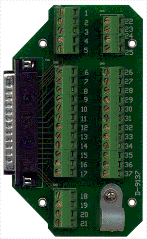
- ACLD‑9137: Direct 37‑pin connector board for simple wiring
- ACLD‑9182: 16‑channel isolated digital input board (500 Vdc isolation)
- ACLD‑9185: 16‑channel SPDT relay output board
- ACLD‑9188: General‑purpose terminal board for 37‑pin D‑sub interface
### 6. Installation & Setup
System Requirements:
- IBM PC/AT or compatible with available ISA slot
- DOS or Windows OS (for software utilities)
Installation Steps:
1. Unpack the card using anti‑static precautions.
2. Verify jumper and DIP switch settings.
3. Insert the card into an available ISA slot.
4. Configure base I/O address (default 0x220) via DIP switch SW1.
5. Set DMA channel (JP7/JP8) and IRQ level (JP5).
6. Configure analog input mode (JP3: SE/DIFF).
7. Select trigger source (JP4: internal/external).
8. Set D/A reference voltage (JP1, JP2).
9. Connect external signals via CN1–CN3.
Mounting Options:
- Standard ISA slot mounting with rear‑panel D‑sub connector.
Configuration:
- Base Address Range: 0x200–0x3FF
- Jumper‑selectable DMA (CH1/CH3) and IRQ (3–15)
- Internal/external trigger and clock source selection
### 7. Performance & Capabilities
A/D Conversion:
- 12‑bit resolution, 8 µs conversion time
- 100 kS/s single‑channel throughput
- 20 kS/s multiplexed throughput
- Programmable gain and range for precise scaling
- Software, pacer, or external triggering
D/A Conversion:
- 12‑bit resolution, 30 µs settling time
- 0–5 V or 0–10 V unipolar output
- ±5 mA drive capability
- Double‑buffered for glitch‑free updates
Digital I/O:
- 16 input and 16 output channels
- TTL/DTL compatible
- Suitable for control, status monitoring, and relay driving
Timer/Counter:
- 8254‑based, 3 independent 16‑bit counters
- Two cascaded counters for A/D pacer (32‑bit)
- User‑programmable counter for event timing or frequency generation
Limitations:
- ISA bus interface (legacy systems)
- Multiplexed A/D sampling limited to 20 kHz for HG model
- Unipolar/bipolar range selection requires jumper configuration
### 8. Standards & Compliance
- Bus Standard: ISA (AT‑Bus)
- Electrical Compliance: TTL/DTL compatible I/O
- Environmental:
- Operating: 0–55 °C
- Storage: –20–80 °C
- Humidity: 5–95% non‑condensing
- Safety: Overvoltage protection ±35 V continuous on analog inputs
- Quality Assurance: Manufactured under ADLINK’s ISO‑certified processes
- Software Standards: Compatible with LabVIEW, Borland C/C++, Visual C++, and Windows SDKs
### 9. Additional Information
Calibration:
- Six on‑board variable resistors (VRs) for fine adjustment:
- VR1: A/D bipolar offset
- VR2: A/D full‑scale
- VR3: D/A CH1 full‑scale
- VR4: D/A CH2 full‑scale
- VR5: A/D amplifier offset
- VR6: A/D unipolar offset
- Calibration utilities provided on software disk
- Recommended equipment: 5½‑digit multimeter and precision voltage source
Software Support:
- C Language Library: 23 functions covering A/D, D/A, DIO, and timer operations
- LabVIEW Driver: ACLS‑LVIEW for Windows 95/98/NT
- Windows SDK: ACLS‑DLL2 for VC++, VB, Delphi
- Demo Programs: AD_DEMO1–4, DA_DEMO, DI_DEMO, DO_DEMO, TMR_DEMO
Warranty:
- 1‑year limited warranty against defects in materials and workmanship
- Excludes misuse, unauthorized modification, or operation beyond specifications
- Repair or replacement at ADLINK’s discretion
Support & Contact:
ADLINK Technology Inc.
9F, No. 166, Jian Yi Road, Chungho City, Taipei 235, Taiwan, R.O.C.
Tel: +886‑2‑82265877 Fax: +886‑2‑82265717
Web: [www.adlink.com.tw](http://www.adlink.com.tw)
Email: service@adlink.com.tw | nudaq@adlink.com.tw
Maintenance:
- Periodic calibration recommended for precision applications
- Keep card free from dust and static discharge
- Store in anti‑static packaging when not in use
Updates:
- Firmware and driver updates available via ADLINK support portal
- Software libraries periodically revised for new OS compatibility
### Summary
The ADLINK ACL‑8112HG is a robust, high‑gain, multifunction data acquisition card engineered for precision analog and digital measurement tasks. With its 12‑bit resolution, programmable gain amplifier, and flexible triggering and transfer modes, it provides a complete solution for laboratory, industrial, and embedded data acquisition systems. Its combination of analog, digital, and timing functions on a single ISA card delivers cost‑effective, high‑accuracy performance for legacy PC‑based control and monitoring applications.

### 1. Product Overview
Product Name: ACL‑8112HG
Model: ACL‑8112HG
Series: ACL‑8112 Series (Enhanced Multi‑Function Data Acquisition Cards)
Article Number: ACL‑8112HG
Manufacturer: ADLINK Technology Inc.
Trademark: NuDAQ®
Product Description:
The ADLINK ACL‑8112HG is a high‑performance, high‑speed, multifunction data acquisition (DAQ) card designed for IBM PC/AT and compatible systems. It integrates analog‑to‑digital (A/D) conversion, digital‑to‑analog (D/A) conversion, digital input/output (DIO), and timer/counter functions on a single half‑size ISA card. The “HG” variant (High Gain) includes a programmable instrumentation amplifier for low‑level signal measurement, making it ideal for precision applications such as thermocouple and sensor data acquisition.
### 2. Key Features
- Bus Interface: AT‑Bus (ISA)
- Analog Inputs: 16 single‑ended or 8 differential channels
- Analog Outputs: Two 12‑bit double‑buffered D/A channels
- Digital I/O: 16 digital inputs and 16 digital outputs (TTL/DTL compatible)
- Resolution: 12‑bit A/D and 12‑bit D/A
- Sampling Rate: Up to 100 kS/s (single channel)
- Programmable Gain:
- High‑gain programmable amplifier with 8 gain levels: ×0.5, ×1, ×5, ×10, ×50, ×100, ×500, ×1000
- Input Range (Programmable):
- Bipolar: ±10V, ±5V, ±1V, ±500mV, ±100mV, ±50mV, ±10mV, ±5mV
- Unipolar: 0–10V, 0–1V, 0–0.1V, 0–0.01V
- Trigger Modes: Software, internal pacer (timer), or external trigger
- Data Transfer Modes: Polling, DMA, or interrupt‑driven
- Timer/Counter:
- 8254 programmable interval timer with three 16‑bit counters
- Two cascaded counters for A/D pacer (32‑bit timer, 2 MHz base)
- One 16‑bit general‑purpose counter
- Interrupts: 9 selectable IRQ levels (IRQ3, 5–7, 9–12, 15)
- DMA Channels: Selectable CH1 or CH3
- Power Supply: On‑board DC/DC converter for stable analog power
- Connectors:
- 37‑pin D‑type female connector (analog I/O, counter/timer)
- Two 20‑pin IDC connectors (digital I/O)
- Form Factor: Half‑size ISA card (compact design)
- Software Support: C‑language library, DOS utilities, LabVIEW driver, and Windows SDK (ACLS‑DLL2)
### 3. Technical Specifications
Analog Input (A/D):
- Converter Type: ADS774 or equivalent, successive approximation
- Resolution: 12 bits
- Channels: 16 SE or 8 DIFF
- Input Impedance: 10 MΩ
- Conversion Time: 8 µs
- Overvoltage Protection: ±35V continuous
- Accuracy (ACL‑8112HG):
- Gain ×0.5, ×1: ±0.01% FSR ±1 LSB
- Gain ×5, ×10: ±0.02% FSR ±1 LSB
- Gain ×50, ×100: ±0.04% FSR ±1 LSB
- Gain ×500, ×1000: ±0.04% FSR ±1 LSB
- Sampling Rate:
- 100 kHz max (single channel)
- 20 kHz max (multiplexed)
- Trigger Modes: Software, pacer, external
- Data Transfer: Polling, DMA, interrupt
Analog Output (D/A):
- Converter: DAC7541 or equivalent
- Channels: 2 (double‑buffered)
- Resolution: 12 bits
- Output Range:
- Internal reference: 0–5V or 0–10V (unipolar)
- External reference: ±10V max
- Settling Time: 30 µs
- Linearity: ±½ LSB
- Output Drive: ±5 mA max
Digital I/O:
- Channels: 16 inputs, 16 outputs (TTL compatible)
- Input Voltage:
- Low ≤ 0.8V, High ≥ 2.0V
- Output Voltage:
- Low ≤ 0.4V @ 8 mA sink
- High ≥ 2.4V @ 0.4 mA source
Timer/Counter:
- Device: Intel/NEC 8254
- Counters: 3 × 16‑bit
- A/D Pacer: Two cascaded counters (32‑bit)
- Base Clock: 2 MHz
- Output Frequency: 0.00046 Hz – 100 kHz
- Counter 0: User‑programmable (event counting, frequency generation)
General:
- I/O Base Address: 16 consecutive locations (default 0x220)
- IRQ Levels: 3, 5–7, 9–12, 15
- DMA Channels: 1 or 3 (jumper‑selectable)
- Operating Temperature: 0–55 °C
- Storage Temperature: –20–80 °C
- Humidity: 5–95% non‑condensing
- Power Consumption:
- +5 V @ 430 mA typical
- +12 V @ 150 mA typical
- Dimensions: 162 mm (L) × 115 mm (W)
- Weight: Approx. 200 g (typical board weight)
### 4. Functionality
Operation Principle:
The ACL‑8112HG performs high‑speed data acquisition by converting analog signals into 12‑bit digital values using a successive‑approximation A/D converter. The programmable gain amplifier allows precise scaling of low‑level signals. The card supports both unipolar and bipolar input ranges, selectable via software or jumpers.
Use Cases & Applications:
- Industrial process monitoring and control
- Laboratory instrumentation and test automation
- Thermocouple and sensor signal acquisition
- Energy management and environmental monitoring
- Event counting, pulse width, and frequency measurement
- Waveform generation and control signal output
- Security and annunciation systems
Compatibility:
- IBM PC/AT and compatible ISA‑bus systems
- Supported operating systems: DOS, Windows 3.1/95/98/NT (via SDK)
- Software environments: C/C++, Visual Basic, Delphi, LabVIEW
### 5. Components & Accessories
Included Items:
- ACL‑8112HG DAQ card
- ADLINK CD (utilities, drivers, libraries)
- User’s Manual
Connectors:
- CN1: 20‑pin IDC (Digital Output)
- CN2: 20‑pin IDC (Digital Input)
- CN3: 37‑pin D‑type female (Analog I/O, Timer/Counter)
Optional Daughter Boards:
- ACLD‑8125: 37‑pin thermocouple input board with cold‑junction compensation (CJC)
- ACLD‑9137: Direct 37‑pin connector board for simple wiring
- ACLD‑9182: 16‑channel isolated digital input board (500 Vdc isolation)
- ACLD‑9185: 16‑channel SPDT relay output board
- ACLD‑9188: General‑purpose terminal board for 37‑pin D‑sub interface
### 6. Installation & Setup
System Requirements:
- IBM PC/AT or compatible with available ISA slot
- DOS or Windows OS (for software utilities)
Installation Steps:
1. Unpack the card using anti‑static precautions.
2. Verify jumper and DIP switch settings.
3. Insert the card into an available ISA slot.
4. Configure base I/O address (default 0x220) via DIP switch SW1.
5. Set DMA channel (JP7/JP8) and IRQ level (JP5).
6. Configure analog input mode (JP3: SE/DIFF).
7. Select trigger source (JP4: internal/external).
8. Set D/A reference voltage (JP1, JP2).
9. Connect external signals via CN1–CN3.
Mounting Options:
- Standard ISA slot mounting with rear‑panel D‑sub connector.
Configuration:
- Base Address Range: 0x200–0x3FF
- Jumper‑selectable DMA (CH1/CH3) and IRQ (3–15)
- Internal/external trigger and clock source selection
### 7. Performance & Capabilities
A/D Conversion:
- 12‑bit resolution, 8 µs conversion time
- 100 kS/s single‑channel throughput
- 20 kS/s multiplexed throughput
- Programmable gain and range for precise scaling
- Software, pacer, or external triggering
D/A Conversion:
- 12‑bit resolution, 30 µs settling time
- 0–5 V or 0–10 V unipolar output
- ±5 mA drive capability
- Double‑buffered for glitch‑free updates
Digital I/O:
- 16 input and 16 output channels
- TTL/DTL compatible
- Suitable for control, status monitoring, and relay driving
Timer/Counter:
- 8254‑based, 3 independent 16‑bit counters
- Two cascaded counters for A/D pacer (32‑bit)
- User‑programmable counter for event timing or frequency generation
Limitations:
- ISA bus interface (legacy systems)
- Multiplexed A/D sampling limited to 20 kHz for HG model
- Unipolar/bipolar range selection requires jumper configuration
### 8. Standards & Compliance
- Bus Standard: ISA (AT‑Bus)
- Electrical Compliance: TTL/DTL compatible I/O
- Environmental:
- Operating: 0–55 °C
- Storage: –20–80 °C
- Humidity: 5–95% non‑condensing
- Safety: Overvoltage protection ±35 V continuous on analog inputs
- Quality Assurance: Manufactured under ADLINK’s ISO‑certified processes
- Software Standards: Compatible with LabVIEW, Borland C/C++, Visual C++, and Windows SDKs
### 9. Additional Information
Calibration:
- Six on‑board variable resistors (VRs) for fine adjustment:
- VR1: A/D bipolar offset
- VR2: A/D full‑scale
- VR3: D/A CH1 full‑scale
- VR4: D/A CH2 full‑scale
- VR5: A/D amplifier offset
- VR6: A/D unipolar offset
- Calibration utilities provided on software disk
- Recommended equipment: 5½‑digit multimeter and precision voltage source
Software Support:
- C Language Library: 23 functions covering A/D, D/A, DIO, and timer operations
- LabVIEW Driver: ACLS‑LVIEW for Windows 95/98/NT
- Windows SDK: ACLS‑DLL2 for VC++, VB, Delphi
- Demo Programs: AD_DEMO1–4, DA_DEMO, DI_DEMO, DO_DEMO, TMR_DEMO
Warranty:
- 1‑year limited warranty against defects in materials and workmanship
- Excludes misuse, unauthorized modification, or operation beyond specifications
- Repair or replacement at ADLINK’s discretion
Support & Contact:
ADLINK Technology Inc.
9F, No. 166, Jian Yi Road, Chungho City, Taipei 235, Taiwan, R.O.C.
Tel: +886‑2‑82265877 Fax: +886‑2‑82265717
Web: [www.adlink.com.tw](http://www.adlink.com.tw)
Email: service@adlink.com.tw | nudaq@adlink.com.tw
Maintenance:
- Periodic calibration recommended for precision applications
- Keep card free from dust and static discharge
- Store in anti‑static packaging when not in use
Updates:
- Firmware and driver updates available via ADLINK support portal
- Software libraries periodically revised for new OS compatibility
### Summary
The ADLINK ACL‑8112HG is a robust, high‑gain, multifunction data acquisition card engineered for precision analog and digital measurement tasks. With its 12‑bit resolution, programmable gain amplifier, and flexible triggering and transfer modes, it provides a complete solution for laboratory, industrial, and embedded data acquisition systems. Its combination of analog, digital, and timing functions on a single ISA card delivers cost‑effective, high‑accuracy performance for legacy PC‑based control and monitoring applications.
-
A8112 Series Manual.pdf
Manual
- ACLD-8125 - Panel with cold junction compensation
- ACLD-9138-01 - Panel general purpose, 2*20 small screw terminal
- ACLD-9137-01 - Direct 37 small screw terminal
- DIN-37D-01 - 37pin D-type panel DIN rail w/o cable
- ACLD-9182A-01 - isolated 16 DI (DC) panel
- ACLD-9185-01 - isolated 16 DO Relay panel
- ACLD-9188 - Panel for mounting low pass filter etc.
- DIN-20P-01 - 20pin header termination board DIN rail
- ACL-10337 - 2*20 pin to DB 37 slot adapter