ACLD-9881
SUCHEN SIE DIE PASSENDE
INDUSTRIELLE LÖSUNG?
Entdecken Sie Embedded-, Kommunikations- und Automatisierungslösungen für Ihre Anwendung.
- High Channel Density: 32 single‑ended isolated analog input channels for simultaneous multi‑point measurement.
- High Voltage Isolation: Each channel is isolated up to 2500 VDC, protecting the host PC and peripherals from high‑voltage transients.
- 12‑bit Resolution: Successive approximation A/D converter (Burr‑Brown AD574 or equivalent) provides precise digital representation of analog signals.
- Programmable Input Range: Bipolar and unipolar ranges selectable via jumpers and software:
- Bipolar: ±10 V, ±5 V, ±2.5 V, ±1.25 V, ±0.625 V, ±0.3125 V
- Unipolar: 0–10 V, 0–5 V, 0–2.5 V, 0–1.25 V, 0–0.625 V
- Software‑Programmable Gain: Selectable gains of ×1, ×2, ×4, ×8, ×16 for flexible scaling.
- On‑Board Signal Conditioning: RC filter networks per channel for attenuation or current‑to‑voltage conversion.
- Integrated DC‑to‑DC Converters: Provide isolated power for analog circuitry, ensuring stable operation and noise immunity.
- Compact Design: Half‑size ISA card (160 mm × 122 mm) with 4‑layer PCB and dedicated ground plane.
- Over‑Voltage Protection: Continuous protection up to ±35 V on all analog inputs.
- Software Triggered Conversion: A/D conversion initiated by software control for flexible timing.
- Comprehensive Software Support: Includes DOS C/C++ libraries, Windows DLLs (ACLS‑DLL2), and LabVIEW drivers (ACLS‑LVIEW).
- Industrial‑Grade Reliability: Designed for 0 °C – 55 °C operation, 5–95 % RH non‑condensing.
- High Voltage Isolation: Each channel is isolated up to 2500 VDC, protecting the host PC and peripherals from high‑voltage transients.
- 12‑bit Resolution: Successive approximation A/D converter (Burr‑Brown AD574 or equivalent) provides precise digital representation of analog signals.
- Programmable Input Range: Bipolar and unipolar ranges selectable via jumpers and software:
- Bipolar: ±10 V, ±5 V, ±2.5 V, ±1.25 V, ±0.625 V, ±0.3125 V
- Unipolar: 0–10 V, 0–5 V, 0–2.5 V, 0–1.25 V, 0–0.625 V
- Software‑Programmable Gain: Selectable gains of ×1, ×2, ×4, ×8, ×16 for flexible scaling.
- On‑Board Signal Conditioning: RC filter networks per channel for attenuation or current‑to‑voltage conversion.
- Integrated DC‑to‑DC Converters: Provide isolated power for analog circuitry, ensuring stable operation and noise immunity.
- Compact Design: Half‑size ISA card (160 mm × 122 mm) with 4‑layer PCB and dedicated ground plane.
- Over‑Voltage Protection: Continuous protection up to ±35 V on all analog inputs.
- Software Triggered Conversion: A/D conversion initiated by software control for flexible timing.
- Comprehensive Software Support: Includes DOS C/C++ libraries, Windows DLLs (ACLS‑DLL2), and LabVIEW drivers (ACLS‑LVIEW).
- Industrial‑Grade Reliability: Designed for 0 °C – 55 °C operation, 5–95 % RH non‑condensing.
Comprehensive Product Summary: ADI12‑16(PC) / ACL‑8113A Isolated Analog Input Card
### 1. Product Overview
Product Name: ADI12‑16(PC)
Model: ACL‑8113A
Series: NuDAQ ISA‑Bus Data Acquisition Series
Article Number: ADI12‑16(PC)
Manufacturer: ADLINK Technology Inc. (Taipei, Taiwan, R.O.C.)
Form Factor: Half‑size ISA‑bus analog input card
Product Type: 12‑bit, 32‑channel single‑ended isolated analog‑to‑digital (A/D) converter card
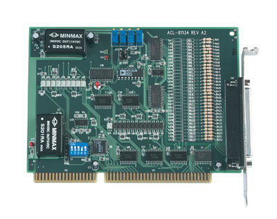
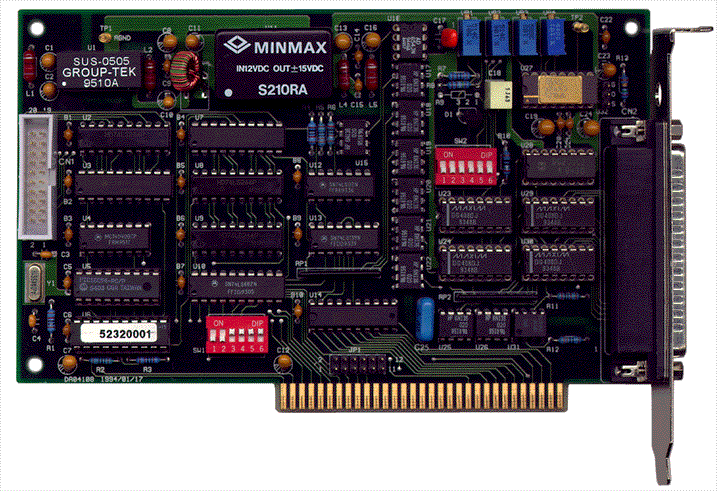
The ADI12‑16(PC), also known as the ACL‑8113A, is a high‑isolation, multi‑channel analog input card designed for PC‑based industrial measurement, monitoring, and data acquisition. It provides 32 isolated single‑ended analog input channels with 12‑bit resolution and a maximum sampling rate of 50 kS/s. The card integrates on‑board signal conditioning, programmable gain control, and dual DC‑to‑DC converters to ensure stable operation and electrical isolation between channels and the system bus.
### 2. Key Features
- High Channel Density: 32 single‑ended isolated analog input channels for simultaneous multi‑point measurement.
- High Voltage Isolation: Each channel is isolated up to 2500 VDC, protecting the host PC and peripherals from high‑voltage transients.
- 12‑bit Resolution: Successive approximation A/D converter (Burr‑Brown AD574 or equivalent) provides precise digital representation of analog signals.
- Programmable Input Range: Bipolar and unipolar ranges selectable via jumpers and software:
- Bipolar: ±10 V, ±5 V, ±2.5 V, ±1.25 V, ±0.625 V, ±0.3125 V
- Unipolar: 0–10 V, 0–5 V, 0–2.5 V, 0–1.25 V, 0–0.625 V
- Software‑Programmable Gain: Selectable gains of ×1, ×2, ×4, ×8, ×16 for flexible scaling.
- On‑Board Signal Conditioning: RC filter networks per channel for attenuation or current‑to‑voltage conversion.
- Integrated DC‑to‑DC Converters: Provide isolated power for analog circuitry, ensuring stable operation and noise immunity.
- Compact Design: Half‑size ISA card (160 mm × 122 mm) with 4‑layer PCB and dedicated ground plane.
- Over‑Voltage Protection: Continuous protection up to ±35 V on all analog inputs.
- Software Triggered Conversion: A/D conversion initiated by software control for flexible timing.
- Comprehensive Software Support: Includes DOS C/C++ libraries, Windows DLLs (ACLS‑DLL2), and LabVIEW drivers (ACLS‑LVIEW).
- Industrial‑Grade Reliability: Designed for 0 °C – 55 °C operation, 5–95 % RH non‑condensing.
### 3. Technical Specifications
Analog Input (A/D):
- Channels: 32 isolated single‑ended
- Resolution: 12 bits
- Conversion Type: Successive approximation (AD574 or equivalent)
- Conversion Rate: Up to 50 kHz (50 kS/s)
- Accuracy: ±0.015 % of reading ± 1 LSB
- Non‑linearity: ±1 bit maximum
- Input Impedance: 10 MΩ typical
- Temperature Coefficient: 5 ppm typical, 15 ppm max
- Over‑voltage Protection: ±35 V continuous
- Trigger Mode: Software trigger only
- Data Transfer: Program‑controlled (polling)
Input Voltage Ranges:
- Bipolar: ±10 V, ±5 V, ±2.5 V, ±1.25 V, ±0.625 V, ±0.3125 V
- Unipolar: 0–10 V, 0–5 V, 0–2.5 V, 0–1.25 V, 0–0.625 V
- Range Selection: Hardware jumpers (JP1, JP2) and software gain control
Electrical Isolation:
- Channel‑to‑channel and channel‑to‑bus isolation: 2500 VDC
- TTL opto‑isolation: up to 5 kV
Connectors:
- 37‑pin female D‑type connector (DB‑37F)
- Pinout: AI0–AI31 (analog inputs), A.GND (analog ground)
Power Requirements:
- +5 V DC @ 960 mA (max)
Physical Characteristics:
- Dimensions: 160 mm (L) × 122 mm (W)
- Form Factor: Half‑size ISA card
- PCB: 4‑layer with ground plane
Environmental:
- Operating Temperature: 0 °C – 55 °C
- Storage Temperature: –20 °C – 80 °C
- Humidity: 5 – 95 % RH, non‑condensing
### 4. Functionality
Operating Principle:
The ACL‑8113A performs analog‑to‑digital conversion using a 12‑bit successive approximation converter. Each input channel is multiplexed through an isolated analog front‑end, conditioned by RC networks, and digitized sequentially under software control. The resulting digital data is stored in two 8‑bit registers (low and high bytes) accessible via I/O port addresses.
Triggering and Data Acquisition:
- Software Trigger: Conversion begins when a value is written to the software trigger register (Base + 12).
- Polling Mechanism: The DRDY (Data Ready) bit indicates conversion completion.
- Data Retrieval: 12‑bit result read from Base + 4 (low byte) and Base + 5 (high byte).
Use Cases and Applications:
- Industrial process monitoring and control
- Sensor and transducer data acquisition
- Waveform and transient analysis
- Vibration and mechanical signal measurement
- Multi‑channel laboratory instrumentation
- Electrical isolation for hazardous or noisy environments
Compatibility:
- ISA‑bus PCs (I/O address range 000h–3F0h)
- Supported OS: DOS, Windows 3.1/95/98/NT
- Supported Software: Borland C/C++, Microsoft C, Visual C++, Visual Basic, Delphi, LabVIEW
### 5. Components & Accessories
Package Contents:
- ACL‑8113A 32‑channel isolated A/D card
- ADLINK CD containing:
- DOS C/C++ library and utilities
- ACLS‑DLL2 Windows development kit
- ACLS‑LVIEW LabVIEW driver package
- Calibration program and documentation
- Printed User’s Manual
Optional Accessories:
- Shielded analog input cables (DB‑37 male to terminal block)
- External terminal boards for sensor wiring
- Additional NuDAQ series cards for system expansion
Connectors and Interfaces:
- DB‑37F Connector Pinout:
- AI0–AI31: Analog input channels
- A.GND: Analog ground reference
- Jumper Settings:
- JP1: Input voltage range (±10 V or ±20 V)
- JP2: Input polarity (Bipolar/Unipolar)
- DIP Switch SW1: Base I/O address selection (default 0x220)
### 6. Installation & Setup
System Requirements:
- IBM‑compatible PC with available ISA slot
- +5 V DC power supply (from system bus)
- Supported OS: DOS or Windows 95/98/NT
Installation Procedure:
1. Unpacking: Handle in an ESD‑safe environment using grounded wrist strap and anti‑static mat.
2. Inspection: Verify no physical damage; ensure all ICs are properly seated.
3. Base Address Configuration:
- Set via 5‑position DIP switch SW1.
- Default base address: 0x220.
- Requires 16 consecutive I/O addresses.
4. Input Range Configuration:
- JP1 selects ±10 V or ±20 V range.
- JP2 selects bipolar (BI) or unipolar (UN) mode.
5. Gain Selection:
- Software‑controlled via A/D range control register (Base + 9).
6. Connector Wiring:
- Connect analog signals to DB‑37F pins AI0–AI31.
- Use A.GND for reference.
7. Driver Installation:
- For DOS: install via `SETUP` from CD (`\NuDAQISA\8113`).
- For Windows: install ACLS‑DLL2 or ACLS‑LVIEW from CD.
Calibration:
- Adjustable via four variable resistors (VR1–VR4):
- VR1: Bipolar offset
- VR2: Bipolar full‑scale
- VR3: Amplifier offset
- VR4: Unipolar full‑scale
- Requires precision voltage source and 6½‑digit multimeter.
### 7. Performance & Capabilities
Sampling Rate: Up to 50 kS/s (software‑controlled)
Resolution: 12 bits (4096 discrete levels)
Accuracy: ±0.015 % of reading ± 1 LSB
Gain Settings: ×1, ×2, ×4, ×8, ×16
Input Impedance: 10 MΩ
Isolation Voltage: 2500 VDC (channel/bus)
Over‑voltage Protection: ±35 V continuous
Power Consumption: 4.8 W (typical)
Operating Range: 0 °C – 55 °C
Limitations:
- Software‑triggered conversion only (no hardware or external trigger).
- Sequential channel sampling (no simultaneous sampling).
- ISA‑bus interface limits use to legacy or industrial PCs.
Performance Optimization:
- Use software polling or timer interrupts for consistent sampling intervals.
- Employ RC filters for noise suppression or current sensing.
- Calibrate periodically for maximum accuracy.
### 8. Standards & Compliance
Electrical and Safety:
- Channel‑to‑bus isolation: 2500 VDC
- TTL opto‑isolation: 5 kV maximum
- Over‑voltage protection: ±35 V continuous
Environmental Compliance:
- Designed for industrial temperature and humidity ranges
- Non‑condensing operation
Software and Interface Standards:
- ISA‑bus compatible (I/O address 000h–3F0h)
- Compatible with standard PC BIOS and DOS/Windows environments
- Supports LabVIEW VI integration via ACLS‑LVIEW
Certifications:
- Manufactured under ADLINK quality control standards
- Conforms to industrial data acquisition hardware design practices
### 9. Additional Information
Warranty:
- One‑year limited warranty from date of purchase.
- Covers defects in materials and workmanship.
- Excludes damage from misuse, modification, or operation beyond specifications.
- Warranty service requires proof of purchase; return shipping prepaid.
Technical Support:
- ADLINK Technology Inc.
- Address: 9F, No. 166, Jian Yi Road, Chungho City, Taipei 235, Taiwan, R.O.C.
- Tel: +886‑2‑8226‑5877
- Fax: +886‑2‑8226‑5717
- Web: [www.adlink.com.tw](http://www.adlink.com.tw)
- Email: service@adlink.com.tw (sales/service)
- Technical Support: nudaq@adlink.com.tw
Maintenance:
- Periodic calibration recommended for accuracy.
- Keep card free of dust and moisture.
- Avoid exposure to static discharge during handling.
Software Updates:
- Updated drivers and libraries available via ADLINK website.
- ACLS‑DLL2 and ACLS‑LVIEW require valid license for installation.
Product Lifecycle:
- Legacy ISA‑bus product; supported for industrial and embedded applications.
- Replacement and upgrade options available in PCI and PXI NuDAQ series.
### Summary
The ADI12‑16(PC) / ACL‑8113A is a robust, high‑isolation, 12‑bit analog input card engineered for industrial data acquisition and monitoring. With 32 isolated single‑ended channels, programmable gain, and flexible input ranges, it provides a cost‑effective solution for multi‑channel analog measurement in harsh or electrically noisy environments. Its combination of hardware isolation, software configurability, and comprehensive programming support makes it suitable for laboratory instrumentation, process control, and sensor data collection applications where precision and reliability are critical.

### 1. Product Overview
Product Name: ADI12‑16(PC)
Model: ACL‑8113A
Series: NuDAQ ISA‑Bus Data Acquisition Series
Article Number: ADI12‑16(PC)
Manufacturer: ADLINK Technology Inc. (Taipei, Taiwan, R.O.C.)
Form Factor: Half‑size ISA‑bus analog input card
Product Type: 12‑bit, 32‑channel single‑ended isolated analog‑to‑digital (A/D) converter card
The ADI12‑16(PC), also known as the ACL‑8113A, is a high‑isolation, multi‑channel analog input card designed for PC‑based industrial measurement, monitoring, and data acquisition. It provides 32 isolated single‑ended analog input channels with 12‑bit resolution and a maximum sampling rate of 50 kS/s. The card integrates on‑board signal conditioning, programmable gain control, and dual DC‑to‑DC converters to ensure stable operation and electrical isolation between channels and the system bus.
### 2. Key Features
- High Channel Density: 32 single‑ended isolated analog input channels for simultaneous multi‑point measurement.
- High Voltage Isolation: Each channel is isolated up to 2500 VDC, protecting the host PC and peripherals from high‑voltage transients.
- 12‑bit Resolution: Successive approximation A/D converter (Burr‑Brown AD574 or equivalent) provides precise digital representation of analog signals.
- Programmable Input Range: Bipolar and unipolar ranges selectable via jumpers and software:
- Bipolar: ±10 V, ±5 V, ±2.5 V, ±1.25 V, ±0.625 V, ±0.3125 V
- Unipolar: 0–10 V, 0–5 V, 0–2.5 V, 0–1.25 V, 0–0.625 V
- Software‑Programmable Gain: Selectable gains of ×1, ×2, ×4, ×8, ×16 for flexible scaling.
- On‑Board Signal Conditioning: RC filter networks per channel for attenuation or current‑to‑voltage conversion.
- Integrated DC‑to‑DC Converters: Provide isolated power for analog circuitry, ensuring stable operation and noise immunity.
- Compact Design: Half‑size ISA card (160 mm × 122 mm) with 4‑layer PCB and dedicated ground plane.
- Over‑Voltage Protection: Continuous protection up to ±35 V on all analog inputs.
- Software Triggered Conversion: A/D conversion initiated by software control for flexible timing.
- Comprehensive Software Support: Includes DOS C/C++ libraries, Windows DLLs (ACLS‑DLL2), and LabVIEW drivers (ACLS‑LVIEW).
- Industrial‑Grade Reliability: Designed for 0 °C – 55 °C operation, 5–95 % RH non‑condensing.
### 3. Technical Specifications
Analog Input (A/D):
- Channels: 32 isolated single‑ended
- Resolution: 12 bits
- Conversion Type: Successive approximation (AD574 or equivalent)
- Conversion Rate: Up to 50 kHz (50 kS/s)
- Accuracy: ±0.015 % of reading ± 1 LSB
- Non‑linearity: ±1 bit maximum
- Input Impedance: 10 MΩ typical
- Temperature Coefficient: 5 ppm typical, 15 ppm max
- Over‑voltage Protection: ±35 V continuous
- Trigger Mode: Software trigger only
- Data Transfer: Program‑controlled (polling)
Input Voltage Ranges:
- Bipolar: ±10 V, ±5 V, ±2.5 V, ±1.25 V, ±0.625 V, ±0.3125 V
- Unipolar: 0–10 V, 0–5 V, 0–2.5 V, 0–1.25 V, 0–0.625 V
- Range Selection: Hardware jumpers (JP1, JP2) and software gain control
Electrical Isolation:
- Channel‑to‑channel and channel‑to‑bus isolation: 2500 VDC
- TTL opto‑isolation: up to 5 kV
Connectors:
- 37‑pin female D‑type connector (DB‑37F)
- Pinout: AI0–AI31 (analog inputs), A.GND (analog ground)
Power Requirements:
- +5 V DC @ 960 mA (max)
Physical Characteristics:
- Dimensions: 160 mm (L) × 122 mm (W)
- Form Factor: Half‑size ISA card
- PCB: 4‑layer with ground plane
Environmental:
- Operating Temperature: 0 °C – 55 °C
- Storage Temperature: –20 °C – 80 °C
- Humidity: 5 – 95 % RH, non‑condensing
### 4. Functionality
Operating Principle:
The ACL‑8113A performs analog‑to‑digital conversion using a 12‑bit successive approximation converter. Each input channel is multiplexed through an isolated analog front‑end, conditioned by RC networks, and digitized sequentially under software control. The resulting digital data is stored in two 8‑bit registers (low and high bytes) accessible via I/O port addresses.
Triggering and Data Acquisition:
- Software Trigger: Conversion begins when a value is written to the software trigger register (Base + 12).
- Polling Mechanism: The DRDY (Data Ready) bit indicates conversion completion.
- Data Retrieval: 12‑bit result read from Base + 4 (low byte) and Base + 5 (high byte).
Use Cases and Applications:
- Industrial process monitoring and control
- Sensor and transducer data acquisition
- Waveform and transient analysis
- Vibration and mechanical signal measurement
- Multi‑channel laboratory instrumentation
- Electrical isolation for hazardous or noisy environments
Compatibility:
- ISA‑bus PCs (I/O address range 000h–3F0h)
- Supported OS: DOS, Windows 3.1/95/98/NT
- Supported Software: Borland C/C++, Microsoft C, Visual C++, Visual Basic, Delphi, LabVIEW
### 5. Components & Accessories
Package Contents:
- ACL‑8113A 32‑channel isolated A/D card
- ADLINK CD containing:
- DOS C/C++ library and utilities
- ACLS‑DLL2 Windows development kit
- ACLS‑LVIEW LabVIEW driver package
- Calibration program and documentation
- Printed User’s Manual
Optional Accessories:
- Shielded analog input cables (DB‑37 male to terminal block)
- External terminal boards for sensor wiring
- Additional NuDAQ series cards for system expansion
Connectors and Interfaces:
- DB‑37F Connector Pinout:
- AI0–AI31: Analog input channels
- A.GND: Analog ground reference
- Jumper Settings:
- JP1: Input voltage range (±10 V or ±20 V)
- JP2: Input polarity (Bipolar/Unipolar)
- DIP Switch SW1: Base I/O address selection (default 0x220)
### 6. Installation & Setup
System Requirements:
- IBM‑compatible PC with available ISA slot
- +5 V DC power supply (from system bus)
- Supported OS: DOS or Windows 95/98/NT
Installation Procedure:
1. Unpacking: Handle in an ESD‑safe environment using grounded wrist strap and anti‑static mat.
2. Inspection: Verify no physical damage; ensure all ICs are properly seated.
3. Base Address Configuration:
- Set via 5‑position DIP switch SW1.
- Default base address: 0x220.
- Requires 16 consecutive I/O addresses.
4. Input Range Configuration:
- JP1 selects ±10 V or ±20 V range.
- JP2 selects bipolar (BI) or unipolar (UN) mode.
5. Gain Selection:
- Software‑controlled via A/D range control register (Base + 9).
6. Connector Wiring:
- Connect analog signals to DB‑37F pins AI0–AI31.
- Use A.GND for reference.
7. Driver Installation:
- For DOS: install via `SETUP` from CD (`\NuDAQISA\8113`).
- For Windows: install ACLS‑DLL2 or ACLS‑LVIEW from CD.
Calibration:
- Adjustable via four variable resistors (VR1–VR4):
- VR1: Bipolar offset
- VR2: Bipolar full‑scale
- VR3: Amplifier offset
- VR4: Unipolar full‑scale
- Requires precision voltage source and 6½‑digit multimeter.
### 7. Performance & Capabilities
Sampling Rate: Up to 50 kS/s (software‑controlled)
Resolution: 12 bits (4096 discrete levels)
Accuracy: ±0.015 % of reading ± 1 LSB
Gain Settings: ×1, ×2, ×4, ×8, ×16
Input Impedance: 10 MΩ
Isolation Voltage: 2500 VDC (channel/bus)
Over‑voltage Protection: ±35 V continuous
Power Consumption: 4.8 W (typical)
Operating Range: 0 °C – 55 °C
Limitations:
- Software‑triggered conversion only (no hardware or external trigger).
- Sequential channel sampling (no simultaneous sampling).
- ISA‑bus interface limits use to legacy or industrial PCs.
Performance Optimization:
- Use software polling or timer interrupts for consistent sampling intervals.
- Employ RC filters for noise suppression or current sensing.
- Calibrate periodically for maximum accuracy.
### 8. Standards & Compliance
Electrical and Safety:
- Channel‑to‑bus isolation: 2500 VDC
- TTL opto‑isolation: 5 kV maximum
- Over‑voltage protection: ±35 V continuous
Environmental Compliance:
- Designed for industrial temperature and humidity ranges
- Non‑condensing operation
Software and Interface Standards:
- ISA‑bus compatible (I/O address 000h–3F0h)
- Compatible with standard PC BIOS and DOS/Windows environments
- Supports LabVIEW VI integration via ACLS‑LVIEW
Certifications:
- Manufactured under ADLINK quality control standards
- Conforms to industrial data acquisition hardware design practices
### 9. Additional Information
Warranty:
- One‑year limited warranty from date of purchase.
- Covers defects in materials and workmanship.
- Excludes damage from misuse, modification, or operation beyond specifications.
- Warranty service requires proof of purchase; return shipping prepaid.
Technical Support:
- ADLINK Technology Inc.
- Address: 9F, No. 166, Jian Yi Road, Chungho City, Taipei 235, Taiwan, R.O.C.
- Tel: +886‑2‑8226‑5877
- Fax: +886‑2‑8226‑5717
- Web: [www.adlink.com.tw](http://www.adlink.com.tw)
- Email: service@adlink.com.tw (sales/service)
- Technical Support: nudaq@adlink.com.tw
Maintenance:
- Periodic calibration recommended for accuracy.
- Keep card free of dust and moisture.
- Avoid exposure to static discharge during handling.
Software Updates:
- Updated drivers and libraries available via ADLINK website.
- ACLS‑DLL2 and ACLS‑LVIEW require valid license for installation.
Product Lifecycle:
- Legacy ISA‑bus product; supported for industrial and embedded applications.
- Replacement and upgrade options available in PCI and PXI NuDAQ series.
### Summary
The ADI12‑16(PC) / ACL‑8113A is a robust, high‑isolation, 12‑bit analog input card engineered for industrial data acquisition and monitoring. With 32 isolated single‑ended channels, programmable gain, and flexible input ranges, it provides a cost‑effective solution for multi‑channel analog measurement in harsh or electrically noisy environments. Its combination of hardware isolation, software configurability, and comprehensive programming support makes it suitable for laboratory instrumentation, process control, and sensor data collection applications where precision and reliability are critical.
-
A8113 Manual.PDF
Manual
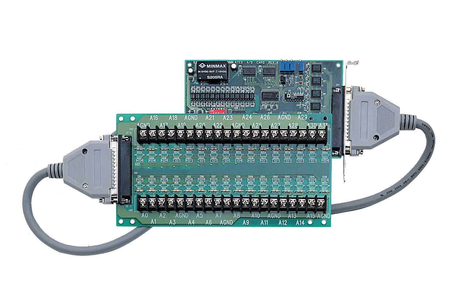
- ACLD-9881 - Panel for mounting low pass filter etc., incl. ACL-10137-1
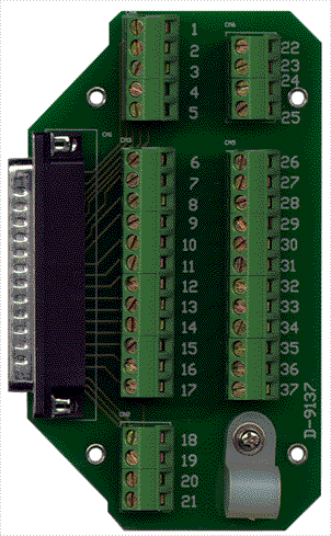
- ACLD-9137-01 - Direct 37 small screw terminal
- DIN-37D-01 - 37pin D-type panel DIN rail w/o cable