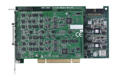
DIN-68S-01
SUCHEN SIE DIE PASSENDE
INDUSTRIELLE LÖSUNG?
Entdecken Sie Embedded-, Kommunikations- und Automatisierungslösungen für Ihre Anwendung.
- High-Speed Analog Output:
- 4 analog output channels, 12-bit resolution, up to 1 MS/s update rate.
- Programmable output ranges: ±10 V, 0–10 V, or external reference (±AOEXTREF).
- Hardware-based arbitrary waveform generation with onboard 8K-sample FIFO.
- Analog Input Capability:
- 8 single-ended analog input channels, 14-bit resolution, up to 400 kS/s sampling rate.
- Bipolar (±10 V) and unipolar (0–10 V) input ranges.
- Onboard 2K-sample A/D FIFO buffer.
- Digital I/O and Counter Functions:
- 24-channel TTL/CMOS-compatible digital I/O (8255 programmable).
- 2-channel, 16-bit general-purpose timer/counter with 40 MHz base clock.
- Triggering and Synchronization:
- Supports software, external digital, and analog triggers.
- System Synchronization Interface (SSI) for multi-card synchronization.
- Post-trigger, delay-trigger, and retrigger modes for both A/D and D/A operations.
- Auto-Calibration:
- Fully automatic internal calibration using a 5 V reference (±2 ppm/°C).
- No external reference required for calibration.
- Bus Interface and Compatibility:
- 32-bit PCI bus (3.3 V or 5 V signaling).
- Plug-and-play configuration with automatic IRQ and address assignment.
- Software and OS Support:
- Drivers for Windows 7/8 (x86/x64) and Linux.
- SDKs for LabVIEW, MATLAB, C/C++, Visual Basic, and Visual Studio.NET.
- AD-Logger utility for data logging and visualization.
- Robust Design:
- Short-circuit protection, ±30 V overvoltage protection on inputs.
- Compact PCI form factor with 68-pin VHDCI connector.
- 4 analog output channels, 12-bit resolution, up to 1 MS/s update rate.
- Programmable output ranges: ±10 V, 0–10 V, or external reference (±AOEXTREF).
- Hardware-based arbitrary waveform generation with onboard 8K-sample FIFO.
- Analog Input Capability:
- 8 single-ended analog input channels, 14-bit resolution, up to 400 kS/s sampling rate.
- Bipolar (±10 V) and unipolar (0–10 V) input ranges.
- Onboard 2K-sample A/D FIFO buffer.
- Digital I/O and Counter Functions:
- 24-channel TTL/CMOS-compatible digital I/O (8255 programmable).
- 2-channel, 16-bit general-purpose timer/counter with 40 MHz base clock.
- Triggering and Synchronization:
- Supports software, external digital, and analog triggers.
- System Synchronization Interface (SSI) for multi-card synchronization.
- Post-trigger, delay-trigger, and retrigger modes for both A/D and D/A operations.
- Auto-Calibration:
- Fully automatic internal calibration using a 5 V reference (±2 ppm/°C).
- No external reference required for calibration.
- Bus Interface and Compatibility:
- 32-bit PCI bus (3.3 V or 5 V signaling).
- Plug-and-play configuration with automatic IRQ and address assignment.
- Software and OS Support:
- Drivers for Windows 7/8 (x86/x64) and Linux.
- SDKs for LabVIEW, MATLAB, C/C++, Visual Basic, and Visual Studio.NET.
- AD-Logger utility for data logging and visualization.
- Robust Design:
- Short-circuit protection, ±30 V overvoltage protection on inputs.
- Compact PCI form factor with 68-pin VHDCI connector.
Comprehensive Product Summary: ADLINK DAQ-2501 PCI Data Acquisition Card
### 1. Product Overview
Product Name: DAQ-2501
Model Number: DAQ-2501
Series: NuDAQ / DAQ-2500 Series (also part of PXI/DAQ/DAQe-2500 family)
Article Number: DAQ-2501
Manufacturer: ADLINK Technology Inc.
Product Type: PCI Bus Multi-Function Data Acquisition (DAQ) Card
Description: 4-channel, 12-bit, 1 MS/s analog output and 8-channel, 14-bit, 400 kS/s analog input multifunction DAQ card with digital I/O, counters, and auto-calibration.
The ADLINK DAQ-2501 is a high-performance PCI-based data acquisition card designed for simultaneous analog waveform generation and data acquisition. It integrates analog output, analog input, digital I/O, and timing/counter functions into a single board, providing a versatile platform for laboratory automation, industrial process control, and signal analysis applications.
### 2. Key Features
- High-Speed Analog Output:
- 4 analog output channels, 12-bit resolution, up to 1 MS/s update rate.
- Programmable output ranges: ±10 V, 0–10 V, or external reference (±AOEXTREF).
- Hardware-based arbitrary waveform generation with onboard 8K-sample FIFO.
- Analog Input Capability:
- 8 single-ended analog input channels, 14-bit resolution, up to 400 kS/s sampling rate.
- Bipolar (±10 V) and unipolar (0–10 V) input ranges.
- Onboard 2K-sample A/D FIFO buffer.
- Digital I/O and Counter Functions:
- 24-channel TTL/CMOS-compatible digital I/O (8255 programmable).
- 2-channel, 16-bit general-purpose timer/counter with 40 MHz base clock.
- Triggering and Synchronization:
- Supports software, external digital, and analog triggers.
- System Synchronization Interface (SSI) for multi-card synchronization.
- Post-trigger, delay-trigger, and retrigger modes for both A/D and D/A operations.
- Auto-Calibration:
- Fully automatic internal calibration using a 5 V reference (±2 ppm/°C).
- No external reference required for calibration.
- Bus Interface and Compatibility:
- 32-bit PCI bus (3.3 V or 5 V signaling).
- Plug-and-play configuration with automatic IRQ and address assignment.
- Software and OS Support:
- Drivers for Windows 7/8 (x86/x64) and Linux.
- SDKs for LabVIEW, MATLAB, C/C++, Visual Basic, and Visual Studio.NET.
- AD-Logger utility for data logging and visualization.
- Robust Design:
- Short-circuit protection, ±30 V overvoltage protection on inputs.
- Compact PCI form factor with 68-pin VHDCI connector.
### 3. Technical Specifications
Analog Output (AO):
- Channels: 4 voltage outputs
- Resolution: 12-bit
- Output Ranges: 0–10 V, ±10 V, 0–AOEXTREF, ±AOEXTREF
- Maximum Update Rate: 1 MS/s
- Slew Rate: 20 V/μs
- Settling Time: 3 μs to ±0.5 LSB
- Offset Error: ±8 mV
- Gain Error: ±0.04% of full-scale output
- Output Drive: ±5 mA
- Load Stability: Up to 1500 pF passive load
- FIFO Buffer: 8K samples
- Data Transfer: Programmed I/O, scatter-gather DMA
- Trigger Sources: Software, external analog/digital, SSI bus
- Trigger Modes: Post-trigger, delay-trigger, repeated trigger
Analog Input (AI):
- Channels: 8 single-ended
- Resolution: 14-bit, no missing codes
- Sampling Rate: 400 kS/s max
- Input Ranges: ±10 V (bipolar), 0–10 V (unipolar)
- Offset Error: ±4 mV
- Gain Error: ±0.1% of FSR
- Input Impedance: 1 GΩ / 6 pF
- Overvoltage Protection: ±30 V (power on), ±15 V (power off)
- Coupling: DC
- FIFO Buffer: 2K samples
- Trigger Sources: Software, external analog/digital, SSI bus
- Data Transfer: Polling, scatter-gather DMA
Digital I/O:
- Channels: 24 (8255 programmable I/O)
- Logic Compatibility: 5 V TTL
- Data Transfer: Programmed I/O
Timer/Counter:
- Channels: 2
- Resolution: 16-bit
- Compatibility: 5 V TTL
- Base Clock: 40 MHz internal, external up to 10 MHz
General Specifications:
- Auto Calibration: Yes (+5 V reference, ±2 ppm/°C)
- Dimensions: 175 mm × 107 mm (6.82" × 4.17")
- Connector: 68-pin VHDCI female
- Operating Temperature: 0°C to 55°C
- Storage Temperature: -20°C to 70°C
- Humidity: 5–95%, non-condensing
- Power Requirements: +5 V @ 1.6 A typical
- Weight: Approx. 250 g
### 4. Functionality
The DAQ-2501 integrates multiple data acquisition functions into a single PCI card:
- Analog Output (D/A Conversion):
Generates precise voltage waveforms using 12-bit DACs. Supports hardware-timed waveform generation with internal/external clocking. Each channel can operate independently with programmable reference and polarity.
- Analog Input (A/D Conversion):
Captures analog signals with 14-bit resolution. Supports software polling or hardware-timed acquisition with DMA transfer for high-speed data throughput.
- Digital I/O:
24 programmable lines for control, monitoring, or synchronization with external devices. Each port (A, B, C) can be configured as input or output.
- Timer/Counter:
Two 16-bit counters for event counting, frequency measurement, or pulse generation. Supports multiple modes including gated counting, pulse-width measurement, and triggered pulse generation.
- Triggering:
Flexible triggering system with software, analog, and digital sources. Supports pre-trigger, post-trigger, delay-trigger, and retrigger modes for both input and output operations.
- Synchronization:
SSI bus allows multiple DAQ-2500 series cards to operate in synchronized mode for multi-channel or distributed measurement systems.
Typical Applications:
- Arbitrary waveform generation
- Transient signal measurement
- Automated test equipment (ATE)
- Process control and monitoring
- Biomedical signal acquisition
- Laboratory automation and instrumentation
Compatibility:
- PCI bus (32-bit, 3.3 V/5 V)
- Compatible with ADLINK terminal boards (DIN-68S-01, ACL-10568-1) and SSI cables (ACL-SSI-2/3/4).
### 5. Components & Accessories
Included Items:
- DAQ-2501 PCI DAQ card
- ADLINK All-in-One CD (drivers, SDKs, utilities)
- Software Installation Guide
- User’s Manual
Optional Accessories:
- Terminal Boards:
- DIN-68S-01 (68-pin screw terminal board)
- ACL-10568-1 (shielded cable assembly)
- Cables:
- ACL-SSI-2/3/4 for synchronization between multiple cards
- Connectors:
- 68-pin VHDCI female connector for analog/digital I/O
### 6. Installation & Setup
System Requirements:
- PCI slot (32-bit, 3.3 V or 5 V signaling)
- Supported OS: Windows 7/8 (x86/x64), Linux
- Minimum 1.6 A @ +5 V power supply
Installation Steps:
1. Power off the PC and install the DAQ-2501 into an available PCI slot.
2. Secure the card and connect the VHDCI cable to the terminal board.
3. Power on the system; the card will be automatically detected (Plug and Play).
4. Install drivers from the ADLINK All-in-One CD.
5. Verify installation using the PCI_SCAN utility.
Configuration:
- No jumpers required; all settings are software-configurable.
- IRQ and I/O addresses are automatically assigned by the BIOS.
- Supports multiple card synchronization via SSI or PXI trigger bus.
### 7. Performance & Capabilities
Analog Output Performance:
- Update Rate: 1 MS/s per channel
- Slew Rate: 20 V/μs
- Settling Time: 3 μs to ±0.5 LSB
- Output Drive: ±5 mA
- Load Capacity: Up to 1500 pF
Analog Input Performance:
- Sampling Rate: 400 kS/s
- Resolution: 14-bit
- Input Impedance: 1 GΩ
- Overvoltage Protection: ±30 V continuous
Digital I/O:
- 24-bit programmable I/O, TTL compatible
- Supports high-speed digital control and monitoring
Timer/Counter:
- 16-bit resolution, up to 10 MHz external clock
- Supports event counting, frequency measurement, and pulse generation
Efficiency and Throughput:
- Scatter-gather DMA for high-speed data transfer
- Bus-mastering DMA minimizes CPU load
- Onboard FIFO buffers (8K for D/A, 2K for A/D) ensure continuous operation
Limitations:
- Analog input limited to 400 kS/s aggregate rate
- Analog output limited to 1 MS/s per channel
- External reference voltage must remain within ±10 V
### 8. Standards & Compliance
- Bus Interface: 32-bit PCI (3.3 V/5 V signaling)
- PXI Compliance: PXI Specification Rev. 2.2 (for PXI variants)
- PCI Express Compliance: x1 lane (for DAQe variants)
- Electrical Standards: TTL/CMOS compatible I/O
- Environmental Compliance:
- Operating Temperature: 0°C to 55°C
- Storage Temperature: -20°C to 70°C
- Humidity: 5–95%, non-condensing
- Safety & EMC: Designed to meet industrial EMC and safety standards
- Calibration Standard: Internal 5 V reference, ±2 ppm/°C stability
### 9. Additional Information
Warranty:
- Standard 2-year limited warranty (1 year in China).
- Covers defects in materials and workmanship.
- Excludes damage from misuse, improper installation, or environmental factors.
Support & Service:
- Global technical support via ADLINK regional offices.
- Email: service@adlinktech.com
- Website: [www.adlinktech.com](http://www.adlinktech.com)
- Toll-Free (US): +1-866-4-ADLINK
Maintenance:
- Recommended warm-up time before calibration: 15 minutes.
- Auto-calibration should be performed periodically for optimal accuracy.
- Store in a dry, temperature-controlled environment when not in use.
Software Updates:
- Driver and SDK updates available from ADLINK’s website.
- Compatible with ADLINK’s D2K-DASK, DAQ-LVIEW PnP, and D2K-OCX libraries.
- Supports integration with LabVIEW, MATLAB, and Visual Studio environments.
Calibration:
- Factory-calibrated prior to shipment.
- Auto-calibration compensates for temperature drift and aging.
- Calibration constants stored in onboard EEPROM (factory and user banks).
Physical & Environmental:
- Compact PCI form factor (175 × 107 mm).
- 68-pin VHDCI connector for all I/O signals.
- Operating humidity: 10–90% non-condensing.
### Summary
The ADLINK DAQ-2501 is a robust, high-precision PCI data acquisition card that combines 4-channel 12-bit analog output, 8-channel 14-bit analog input, 24-channel digital I/O, and dual 16-bit counters into a single, compact board. With its 1 MS/s output rate, 400 kS/s input rate, and advanced triggering and synchronization capabilities, it is ideal for demanding applications such as waveform generation, process control, and automated testing. The card’s fully auto-calibrated design, scatter-gather DMA support, and broad software compatibility make it a versatile and reliable solution for engineers and researchers requiring precise, high-speed data acquisition and signal generation.

### 1. Product Overview
Product Name: DAQ-2501
Model Number: DAQ-2501
Series: NuDAQ / DAQ-2500 Series (also part of PXI/DAQ/DAQe-2500 family)
Article Number: DAQ-2501
Manufacturer: ADLINK Technology Inc.
Product Type: PCI Bus Multi-Function Data Acquisition (DAQ) Card
Description: 4-channel, 12-bit, 1 MS/s analog output and 8-channel, 14-bit, 400 kS/s analog input multifunction DAQ card with digital I/O, counters, and auto-calibration.
The ADLINK DAQ-2501 is a high-performance PCI-based data acquisition card designed for simultaneous analog waveform generation and data acquisition. It integrates analog output, analog input, digital I/O, and timing/counter functions into a single board, providing a versatile platform for laboratory automation, industrial process control, and signal analysis applications.
### 2. Key Features
- High-Speed Analog Output:
- 4 analog output channels, 12-bit resolution, up to 1 MS/s update rate.
- Programmable output ranges: ±10 V, 0–10 V, or external reference (±AOEXTREF).
- Hardware-based arbitrary waveform generation with onboard 8K-sample FIFO.
- Analog Input Capability:
- 8 single-ended analog input channels, 14-bit resolution, up to 400 kS/s sampling rate.
- Bipolar (±10 V) and unipolar (0–10 V) input ranges.
- Onboard 2K-sample A/D FIFO buffer.
- Digital I/O and Counter Functions:
- 24-channel TTL/CMOS-compatible digital I/O (8255 programmable).
- 2-channel, 16-bit general-purpose timer/counter with 40 MHz base clock.
- Triggering and Synchronization:
- Supports software, external digital, and analog triggers.
- System Synchronization Interface (SSI) for multi-card synchronization.
- Post-trigger, delay-trigger, and retrigger modes for both A/D and D/A operations.
- Auto-Calibration:
- Fully automatic internal calibration using a 5 V reference (±2 ppm/°C).
- No external reference required for calibration.
- Bus Interface and Compatibility:
- 32-bit PCI bus (3.3 V or 5 V signaling).
- Plug-and-play configuration with automatic IRQ and address assignment.
- Software and OS Support:
- Drivers for Windows 7/8 (x86/x64) and Linux.
- SDKs for LabVIEW, MATLAB, C/C++, Visual Basic, and Visual Studio.NET.
- AD-Logger utility for data logging and visualization.
- Robust Design:
- Short-circuit protection, ±30 V overvoltage protection on inputs.
- Compact PCI form factor with 68-pin VHDCI connector.
### 3. Technical Specifications
Analog Output (AO):
- Channels: 4 voltage outputs
- Resolution: 12-bit
- Output Ranges: 0–10 V, ±10 V, 0–AOEXTREF, ±AOEXTREF
- Maximum Update Rate: 1 MS/s
- Slew Rate: 20 V/μs
- Settling Time: 3 μs to ±0.5 LSB
- Offset Error: ±8 mV
- Gain Error: ±0.04% of full-scale output
- Output Drive: ±5 mA
- Load Stability: Up to 1500 pF passive load
- FIFO Buffer: 8K samples
- Data Transfer: Programmed I/O, scatter-gather DMA
- Trigger Sources: Software, external analog/digital, SSI bus
- Trigger Modes: Post-trigger, delay-trigger, repeated trigger
Analog Input (AI):
- Channels: 8 single-ended
- Resolution: 14-bit, no missing codes
- Sampling Rate: 400 kS/s max
- Input Ranges: ±10 V (bipolar), 0–10 V (unipolar)
- Offset Error: ±4 mV
- Gain Error: ±0.1% of FSR
- Input Impedance: 1 GΩ / 6 pF
- Overvoltage Protection: ±30 V (power on), ±15 V (power off)
- Coupling: DC
- FIFO Buffer: 2K samples
- Trigger Sources: Software, external analog/digital, SSI bus
- Data Transfer: Polling, scatter-gather DMA
Digital I/O:
- Channels: 24 (8255 programmable I/O)
- Logic Compatibility: 5 V TTL
- Data Transfer: Programmed I/O
Timer/Counter:
- Channels: 2
- Resolution: 16-bit
- Compatibility: 5 V TTL
- Base Clock: 40 MHz internal, external up to 10 MHz
General Specifications:
- Auto Calibration: Yes (+5 V reference, ±2 ppm/°C)
- Dimensions: 175 mm × 107 mm (6.82" × 4.17")
- Connector: 68-pin VHDCI female
- Operating Temperature: 0°C to 55°C
- Storage Temperature: -20°C to 70°C
- Humidity: 5–95%, non-condensing
- Power Requirements: +5 V @ 1.6 A typical
- Weight: Approx. 250 g
### 4. Functionality
The DAQ-2501 integrates multiple data acquisition functions into a single PCI card:
- Analog Output (D/A Conversion):
Generates precise voltage waveforms using 12-bit DACs. Supports hardware-timed waveform generation with internal/external clocking. Each channel can operate independently with programmable reference and polarity.
- Analog Input (A/D Conversion):
Captures analog signals with 14-bit resolution. Supports software polling or hardware-timed acquisition with DMA transfer for high-speed data throughput.
- Digital I/O:
24 programmable lines for control, monitoring, or synchronization with external devices. Each port (A, B, C) can be configured as input or output.
- Timer/Counter:
Two 16-bit counters for event counting, frequency measurement, or pulse generation. Supports multiple modes including gated counting, pulse-width measurement, and triggered pulse generation.
- Triggering:
Flexible triggering system with software, analog, and digital sources. Supports pre-trigger, post-trigger, delay-trigger, and retrigger modes for both input and output operations.
- Synchronization:
SSI bus allows multiple DAQ-2500 series cards to operate in synchronized mode for multi-channel or distributed measurement systems.
Typical Applications:
- Arbitrary waveform generation
- Transient signal measurement
- Automated test equipment (ATE)
- Process control and monitoring
- Biomedical signal acquisition
- Laboratory automation and instrumentation
Compatibility:
- PCI bus (32-bit, 3.3 V/5 V)
- Compatible with ADLINK terminal boards (DIN-68S-01, ACL-10568-1) and SSI cables (ACL-SSI-2/3/4).
### 5. Components & Accessories
Included Items:
- DAQ-2501 PCI DAQ card
- ADLINK All-in-One CD (drivers, SDKs, utilities)
- Software Installation Guide
- User’s Manual
Optional Accessories:
- Terminal Boards:
- DIN-68S-01 (68-pin screw terminal board)
- ACL-10568-1 (shielded cable assembly)
- Cables:
- ACL-SSI-2/3/4 for synchronization between multiple cards
- Connectors:
- 68-pin VHDCI female connector for analog/digital I/O
### 6. Installation & Setup
System Requirements:
- PCI slot (32-bit, 3.3 V or 5 V signaling)
- Supported OS: Windows 7/8 (x86/x64), Linux
- Minimum 1.6 A @ +5 V power supply
Installation Steps:
1. Power off the PC and install the DAQ-2501 into an available PCI slot.
2. Secure the card and connect the VHDCI cable to the terminal board.
3. Power on the system; the card will be automatically detected (Plug and Play).
4. Install drivers from the ADLINK All-in-One CD.
5. Verify installation using the PCI_SCAN utility.
Configuration:
- No jumpers required; all settings are software-configurable.
- IRQ and I/O addresses are automatically assigned by the BIOS.
- Supports multiple card synchronization via SSI or PXI trigger bus.
### 7. Performance & Capabilities
Analog Output Performance:
- Update Rate: 1 MS/s per channel
- Slew Rate: 20 V/μs
- Settling Time: 3 μs to ±0.5 LSB
- Output Drive: ±5 mA
- Load Capacity: Up to 1500 pF
Analog Input Performance:
- Sampling Rate: 400 kS/s
- Resolution: 14-bit
- Input Impedance: 1 GΩ
- Overvoltage Protection: ±30 V continuous
Digital I/O:
- 24-bit programmable I/O, TTL compatible
- Supports high-speed digital control and monitoring
Timer/Counter:
- 16-bit resolution, up to 10 MHz external clock
- Supports event counting, frequency measurement, and pulse generation
Efficiency and Throughput:
- Scatter-gather DMA for high-speed data transfer
- Bus-mastering DMA minimizes CPU load
- Onboard FIFO buffers (8K for D/A, 2K for A/D) ensure continuous operation
Limitations:
- Analog input limited to 400 kS/s aggregate rate
- Analog output limited to 1 MS/s per channel
- External reference voltage must remain within ±10 V
### 8. Standards & Compliance
- Bus Interface: 32-bit PCI (3.3 V/5 V signaling)
- PXI Compliance: PXI Specification Rev. 2.2 (for PXI variants)
- PCI Express Compliance: x1 lane (for DAQe variants)
- Electrical Standards: TTL/CMOS compatible I/O
- Environmental Compliance:
- Operating Temperature: 0°C to 55°C
- Storage Temperature: -20°C to 70°C
- Humidity: 5–95%, non-condensing
- Safety & EMC: Designed to meet industrial EMC and safety standards
- Calibration Standard: Internal 5 V reference, ±2 ppm/°C stability
### 9. Additional Information
Warranty:
- Standard 2-year limited warranty (1 year in China).
- Covers defects in materials and workmanship.
- Excludes damage from misuse, improper installation, or environmental factors.
Support & Service:
- Global technical support via ADLINK regional offices.
- Email: service@adlinktech.com
- Website: [www.adlinktech.com](http://www.adlinktech.com)
- Toll-Free (US): +1-866-4-ADLINK
Maintenance:
- Recommended warm-up time before calibration: 15 minutes.
- Auto-calibration should be performed periodically for optimal accuracy.
- Store in a dry, temperature-controlled environment when not in use.
Software Updates:
- Driver and SDK updates available from ADLINK’s website.
- Compatible with ADLINK’s D2K-DASK, DAQ-LVIEW PnP, and D2K-OCX libraries.
- Supports integration with LabVIEW, MATLAB, and Visual Studio environments.
Calibration:
- Factory-calibrated prior to shipment.
- Auto-calibration compensates for temperature drift and aging.
- Calibration constants stored in onboard EEPROM (factory and user banks).
Physical & Environmental:
- Compact PCI form factor (175 × 107 mm).
- 68-pin VHDCI connector for all I/O signals.
- Operating humidity: 10–90% non-condensing.
### Summary
The ADLINK DAQ-2501 is a robust, high-precision PCI data acquisition card that combines 4-channel 12-bit analog output, 8-channel 14-bit analog input, 24-channel digital I/O, and dual 16-bit counters into a single, compact board. With its 1 MS/s output rate, 400 kS/s input rate, and advanced triggering and synchronization capabilities, it is ideal for demanding applications such as waveform generation, process control, and automated testing. The card’s fully auto-calibrated design, scatter-gather DMA support, and broad software compatibility make it a versatile and reliable solution for engineers and researchers requiring precise, high-speed data acquisition and signal generation.
-
DAQe-2500Series_Datasheet_en_2.pdf
PDF Catalog
-
DAQe-2500Series_Manual.pdf
Manual
- DIN-68S-01 - 68pin SCSI-II termination board DIN rail w/o cable
- ACL-10568-1 - SCSI-VHDCI cable 1m for DAQ series
- ACL-10568-2 - SCSI-VHDCI cable 2m for DAQ series
- ACL-10568-3 - SCSI-VHDCI cable 3m for DAQ series