DIN-68S-01
SUCHEN SIE DIE PASSENDE
INDUSTRIELLE LÖSUNG?
Entdecken Sie Embedded-, Kommunikations- und Automatisierungslösungen für Ihre Anwendung.
- High‑speed analog output: 8 channels, 12‑bit resolution, up to 1 MS/s per channel.
- Analog input capability: 4 single‑ended channels, 14‑bit resolution, up to 400 kS/s sampling rate.
- Simultaneous waveform generation: Hardware‑based arbitrary waveform generation with onboard FIFO buffering.
- Auto‑calibration: Fully automatic internal calibration using a precision 5 V reference (±2 ppm/°C).
- Programmable voltage ranges: Bipolar (±10 V) and unipolar (0–10 V) ranges for both input and output.
- Flexible triggering: Supports software, external digital, external analog, and SSI (System Synchronization Interface) triggers.
- Scatter‑gather DMA: High‑speed data transfer for both A/D and D/A operations with minimal CPU load.
- Digital I/O: 24‑channel TTL/CMOS‑compatible programmable I/O (8255‑compatible).
- Timer/Counter: Two 16‑bit general‑purpose up/down counters with 40 MHz internal or 10 MHz external clock.
- Synchronization: Multiple‑card synchronization via SSI bus or PXI trigger bus.
- Software support: Drivers and SDKs for Windows and Linux; compatible with LabVIEW®, MATLAB®, C/C++, Visual Basic, and .NET.
- Plug‑and‑play PCI configuration: No jumpers required; automatic IRQ and address assignment.
- Compact design: 175 mm × 107 mm PCI form factor with 68‑pin VHDCI connector.
- Analog input capability: 4 single‑ended channels, 14‑bit resolution, up to 400 kS/s sampling rate.
- Simultaneous waveform generation: Hardware‑based arbitrary waveform generation with onboard FIFO buffering.
- Auto‑calibration: Fully automatic internal calibration using a precision 5 V reference (±2 ppm/°C).
- Programmable voltage ranges: Bipolar (±10 V) and unipolar (0–10 V) ranges for both input and output.
- Flexible triggering: Supports software, external digital, external analog, and SSI (System Synchronization Interface) triggers.
- Scatter‑gather DMA: High‑speed data transfer for both A/D and D/A operations with minimal CPU load.
- Digital I/O: 24‑channel TTL/CMOS‑compatible programmable I/O (8255‑compatible).
- Timer/Counter: Two 16‑bit general‑purpose up/down counters with 40 MHz internal or 10 MHz external clock.
- Synchronization: Multiple‑card synchronization via SSI bus or PXI trigger bus.
- Software support: Drivers and SDKs for Windows and Linux; compatible with LabVIEW®, MATLAB®, C/C++, Visual Basic, and .NET.
- Plug‑and‑play PCI configuration: No jumpers required; automatic IRQ and address assignment.
- Compact design: 175 mm × 107 mm PCI form factor with 68‑pin VHDCI connector.
Comprehensive Product Summary: ADLINK DAQ‑2502 PCI Data Acquisition Card
### 1. Product Overview
Product Name: DAQ‑2502
Model: DAQ‑2502
Series: NuDAQ‑2500 / PXI/DAQ/DAQe‑2500 Series
Article Number: DAQ‑2502
Manufacturer: ADLINK Technology Inc.
Product Type: PCI‑bus multifunction data acquisition (DAQ) card with analog output and input capabilities
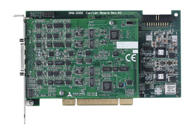
The ADLINK DAQ‑2502 is a high‑performance, 32‑bit PCI‑based multifunction data acquisition card designed for simultaneous analog waveform generation, analog input sampling, digital I/O, and counter/timer operations. It belongs to ADLINK’s NuDAQ‑2500 Series, which also includes PXI and PCI Express (DAQe) variants. The DAQ‑2502 model specifically provides 8 analog output channels and 4 analog input channels, optimized for applications requiring high‑speed, high‑resolution analog signal generation and measurement.
### 2. Key Features
- High‑speed analog output: 8 channels, 12‑bit resolution, up to 1 MS/s per channel.
- Analog input capability: 4 single‑ended channels, 14‑bit resolution, up to 400 kS/s sampling rate.
- Simultaneous waveform generation: Hardware‑based arbitrary waveform generation with onboard FIFO buffering.
- Auto‑calibration: Fully automatic internal calibration using a precision 5 V reference (±2 ppm/°C).
- Programmable voltage ranges: Bipolar (±10 V) and unipolar (0–10 V) ranges for both input and output.
- Flexible triggering: Supports software, external digital, external analog, and SSI (System Synchronization Interface) triggers.
- Scatter‑gather DMA: High‑speed data transfer for both A/D and D/A operations with minimal CPU load.
- Digital I/O: 24‑channel TTL/CMOS‑compatible programmable I/O (8255‑compatible).
- Timer/Counter: Two 16‑bit general‑purpose up/down counters with 40 MHz internal or 10 MHz external clock.
- Synchronization: Multiple‑card synchronization via SSI bus or PXI trigger bus.
- Software support: Drivers and SDKs for Windows and Linux; compatible with LabVIEW®, MATLAB®, C/C++, Visual Basic, and .NET.
- Plug‑and‑play PCI configuration: No jumpers required; automatic IRQ and address assignment.
- Compact design: 175 mm × 107 mm PCI form factor with 68‑pin VHDCI connector.
### 3. Technical Specifications
Analog Output (AO):
- Channels: 8 voltage outputs
- Resolution: 12 bits
- Output ranges: 0–10 V, ±10 V, 0–AOEXTREF, ±AOEXTREF
- Maximum update rate: 1 MS/s
- Slew rate: 20 V/µs
- Settling time: 3 µs to ±0.5 LSB
- Offset error: ±8 mV (after calibration ±2 mV typical)
- Gain error: ±0.04 % of full‑scale (after calibration ±0.02 %)
- Output current drive: ±5 mA
- Load stability: Any passive load up to 1500 pF
- Output impedance: ≤ 0.1 Ω
- Protection: Short‑circuit to ground
- FIFO buffer: 16 k samples
- Data transfer: Programmed I/O or scatter‑gather DMA
Analog Input (AI):
- Channels: 4 single‑ended
- Resolution: 14 bits, no missing codes
- Sampling rate: 400 kS/s maximum
- Input ranges: ±10 V (bipolar), 0–10 V (unipolar)
- Input coupling: DC
- Input impedance: 1 GΩ / 6 pF
- Offset error: ±4 mV (after calibration ±1 mV)
- Gain error: ±0.1 % of FSR (after calibration ±0.02 %)
- Overvoltage protection: ±30 V continuous (power on), ±15 V (power off)
- FIFO buffer: 2 k samples
- Data transfer: Polling or scatter‑gather DMA
Digital I/O:
- Channels: 24 programmable I/O lines (8255‑compatible)
- Logic levels: TTL/CMOS, 5 V compatible
- Input low ≤ 0.8 V, input high ≥ 2.0 V
- Output low ≤ 0.5 V @ 8 mA, output high ≥ 2.7 V @ 400 µA
Timer/Counter:
- Channels: 2 independent 16‑bit up/down counters
- Clock source: Internal 40 MHz or external up to 10 MHz
- Compatibility: TTL/CMOS
- Modes: 8 programmable modes including event counting, pulse generation, and period measurement
General:
- Auto‑calibration: Yes, internal 5 V reference (±2 ppm/°C)
- Dimensions: 175 mm × 107 mm (6.82 in × 4.17 in)
- Connector: 68‑pin VHDCI female (mini‑SCSI type)
- Operating temperature: 0 °C – 55 °C
- Storage temperature: −20 °C – 70 °C
- Humidity: 5 % – 95 %, non‑condensing
- Power requirements: +5 V @ 2.12 A typical
- Bus interface: 32‑bit PCI, 3.3 V/5 V signaling
### 4. Functionality
The DAQ‑2502 integrates multiple data acquisition functions on a single PCI card:
- Analog Output (D/A Conversion):
Generates precise analog voltages or waveforms. Each of the eight 12‑bit DAC channels can operate independently with programmable ranges and reference sources. Hardware‑based waveform generation ensures deterministic timing and minimal CPU overhead.
- Analog Input (A/D Conversion):
Captures analog signals from sensors or test points. The 14‑bit ADC supports software polling or hardware‑timed scanning with programmable trigger modes (post‑trigger, delay‑trigger, retrigger).
- Digital I/O:
Provides 24 TTL‑compatible lines for control, monitoring, or synchronization with external devices.
- Timer/Counter:
Two 16‑bit counters support event counting, frequency measurement, pulse generation, and gating functions.
- Triggering and Synchronization:
Supports software, external digital, and analog triggers, as well as SSI bus synchronization for multi‑card systems.
Typical Applications:
- Arbitrary waveform generation and signal simulation
- Automated test equipment (ATE)
- Process control and industrial automation
- Transient signal measurement
- Laboratory instrumentation and data logging
- Biomedical and biotech measurement systems
Compatibility:
- Operating Systems: Windows 7/8 x86/x64, Linux
- Software Environments: LabVIEW®, MATLAB®, Visual Studio .NET, C/C++, Visual Basic
- Drivers: ADLINK D2K‑DASK, D2K‑DASK/X, DAQ‑LVIEW PnP, D2K‑OCX ActiveX
### 5. Components & Accessories
Included Items:
- DAQ‑2502 PCI multifunction DAQ card
- ADLINK All‑in‑One software CD (drivers, SDKs, utilities)
- Software Installation Guide
- User’s Manual
Optional Accessories:
- DIN‑68S‑01: 68‑pin screw‑terminal board
- ACL‑10568‑1: 68‑pin shielded cable
- ACL‑SSI‑2/3/4: SSI synchronization cables for multi‑card setups
Connectors:
- One 68‑pin VHDCI female connector for analog, digital, and timing I/O
- Pin assignments include AO, AI, DIO, GPTC, AFI, and trigger lines
### 6. Installation & Setup
Requirements:
- Available 32‑bit PCI slot (3.3 V or 5 V signaling)
- Supported OS and driver installation from ADLINK CD
Installation Steps:
1. Power off the host PC and discharge static electricity.
2. Insert the DAQ‑2502 into an available PCI slot.
3. Secure the card and connect the VHDCI cable to external terminal boards.
4. Power on the system; the card is automatically detected (Plug‑and‑Play).
5. Install ADLINK drivers and verify operation using the AD‑Logger utility.
Configuration:
- No jumpers required; all settings are software‑configurable.
- IRQ and base address automatically assigned by BIOS.
- Use ADLINK’s PCI_SCAN utility to verify resource allocation.
Mounting Options:
- Standard PCI slot mounting; compatible with desktop or industrial PCs.
### 7. Performance & Capabilities
Analog Output Performance:
- Update rate: 1 MS/s per channel
- Slew rate: 20 V/µs
- Settling time: 3 µs to ±0.5 LSB
- Output stability: Supports capacitive loads up to 1500 pF
- Waveform generation: Hardware‑controlled with 16 k‑sample FIFO and DMA streaming
Analog Input Performance:
- Sampling rate: 400 kS/s
- Resolution: 14 bits
- Input protection: ±30 V continuous
- FIFO: 2 k samples
- Trigger modes: Post‑trigger, delay‑trigger, retrigger
Digital I/O:
- 24 channels, programmable direction
- 8255‑compatible, TTL/CMOS levels
Timer/Counter:
- 16‑bit resolution, up to 10 MHz external clock
- 8 programmable modes for event counting, pulse generation, and measurement
Efficiency:
- Scatter‑gather DMA minimizes CPU load during high‑speed transfers.
- Auto‑calibration ensures long‑term accuracy without manual adjustment.
Limitations:
- Analog input limited to 400 kS/s aggregate rate.
- Output current limited to ±5 mA per channel.
- External reference voltage must remain within ±10 V.
### 8. Standards & Compliance
- Bus Interface: PCI 2.2 compliant (32‑bit, 33 MHz, 3.3 V/5 V signaling)
- PXI Compliance: PXI specification Rev 2.2 (for PXI variant)
- PCI Express Compliance: x1 lane PCIe (for DAQe variant)
- Electrical Safety: TTL/CMOS logic levels, short‑circuit protected outputs
- Environmental: Operating 0–55 °C, storage −20–70 °C, 5–95 % RH non‑condensing
- Calibration Reference: ±2 ppm/°C temperature coefficient, 6 ppm/1000 hr stability
- Regulatory: CE and FCC Class A (typical for ADLINK industrial cards)
### 9. Additional Information
Warranty:
- Standard limited two‑year warranty (one year in China) from date of shipment.
- Covers manufacturing defects; excludes damage from misuse, improper installation, or environmental factors.
Support & Service:
- Global technical support via ADLINK regional offices (Taiwan, USA, Europe, Singapore, India, China).
- Email: service@adlinktech.com
- Website: [www.adlinktech.com](http://www.adlinktech.com)
Maintenance:
- Recommended warm‑up time before calibration: 15 minutes.
- Periodic auto‑calibration ensures measurement accuracy.
- Store in dry, static‑free environment when not in use.
Software Updates:
- Driver and SDK updates available from ADLINK’s website.
- Compatible with AD‑Logger utility for data logging and diagnostics.
Calibration:
- Factory‑calibrated prior to shipment.
- Auto‑calibration compensates for offset and gain drift using onboard reference.
- Calibration constants stored in EEPROM (factory and user banks).
Documentation:
- User’s Manual (Rev 2.01)
- Part No. 50‑11221‑2000
- Includes detailed pinouts, operation theory, and programming references.
### Summary
The ADLINK DAQ‑2502 is a robust, high‑precision PCI data acquisition card engineered for demanding industrial, laboratory, and research applications. With 8 channels of 12‑bit analog output at 1 MS/s, 4 channels of 14‑bit analog input at 400 kS/s, and comprehensive digital and timing features, it provides a complete solution for waveform generation, signal measurement, and process control. Its auto‑calibration, DMA‑based data transfer, and multi‑card synchronization capabilities make it ideal for high‑speed, high‑accuracy data acquisition systems.
The DAQ‑2502’s combination of performance, flexibility, and software support ensures seamless integration into automated test systems, control environments, and scientific instrumentation platforms.

### 1. Product Overview
Product Name: DAQ‑2502
Model: DAQ‑2502
Series: NuDAQ‑2500 / PXI/DAQ/DAQe‑2500 Series
Article Number: DAQ‑2502
Manufacturer: ADLINK Technology Inc.
Product Type: PCI‑bus multifunction data acquisition (DAQ) card with analog output and input capabilities
The ADLINK DAQ‑2502 is a high‑performance, 32‑bit PCI‑based multifunction data acquisition card designed for simultaneous analog waveform generation, analog input sampling, digital I/O, and counter/timer operations. It belongs to ADLINK’s NuDAQ‑2500 Series, which also includes PXI and PCI Express (DAQe) variants. The DAQ‑2502 model specifically provides 8 analog output channels and 4 analog input channels, optimized for applications requiring high‑speed, high‑resolution analog signal generation and measurement.
### 2. Key Features
- High‑speed analog output: 8 channels, 12‑bit resolution, up to 1 MS/s per channel.
- Analog input capability: 4 single‑ended channels, 14‑bit resolution, up to 400 kS/s sampling rate.
- Simultaneous waveform generation: Hardware‑based arbitrary waveform generation with onboard FIFO buffering.
- Auto‑calibration: Fully automatic internal calibration using a precision 5 V reference (±2 ppm/°C).
- Programmable voltage ranges: Bipolar (±10 V) and unipolar (0–10 V) ranges for both input and output.
- Flexible triggering: Supports software, external digital, external analog, and SSI (System Synchronization Interface) triggers.
- Scatter‑gather DMA: High‑speed data transfer for both A/D and D/A operations with minimal CPU load.
- Digital I/O: 24‑channel TTL/CMOS‑compatible programmable I/O (8255‑compatible).
- Timer/Counter: Two 16‑bit general‑purpose up/down counters with 40 MHz internal or 10 MHz external clock.
- Synchronization: Multiple‑card synchronization via SSI bus or PXI trigger bus.
- Software support: Drivers and SDKs for Windows and Linux; compatible with LabVIEW®, MATLAB®, C/C++, Visual Basic, and .NET.
- Plug‑and‑play PCI configuration: No jumpers required; automatic IRQ and address assignment.
- Compact design: 175 mm × 107 mm PCI form factor with 68‑pin VHDCI connector.
### 3. Technical Specifications
Analog Output (AO):
- Channels: 8 voltage outputs
- Resolution: 12 bits
- Output ranges: 0–10 V, ±10 V, 0–AOEXTREF, ±AOEXTREF
- Maximum update rate: 1 MS/s
- Slew rate: 20 V/µs
- Settling time: 3 µs to ±0.5 LSB
- Offset error: ±8 mV (after calibration ±2 mV typical)
- Gain error: ±0.04 % of full‑scale (after calibration ±0.02 %)
- Output current drive: ±5 mA
- Load stability: Any passive load up to 1500 pF
- Output impedance: ≤ 0.1 Ω
- Protection: Short‑circuit to ground
- FIFO buffer: 16 k samples
- Data transfer: Programmed I/O or scatter‑gather DMA
Analog Input (AI):
- Channels: 4 single‑ended
- Resolution: 14 bits, no missing codes
- Sampling rate: 400 kS/s maximum
- Input ranges: ±10 V (bipolar), 0–10 V (unipolar)
- Input coupling: DC
- Input impedance: 1 GΩ / 6 pF
- Offset error: ±4 mV (after calibration ±1 mV)
- Gain error: ±0.1 % of FSR (after calibration ±0.02 %)
- Overvoltage protection: ±30 V continuous (power on), ±15 V (power off)
- FIFO buffer: 2 k samples
- Data transfer: Polling or scatter‑gather DMA
Digital I/O:
- Channels: 24 programmable I/O lines (8255‑compatible)
- Logic levels: TTL/CMOS, 5 V compatible
- Input low ≤ 0.8 V, input high ≥ 2.0 V
- Output low ≤ 0.5 V @ 8 mA, output high ≥ 2.7 V @ 400 µA
Timer/Counter:
- Channels: 2 independent 16‑bit up/down counters
- Clock source: Internal 40 MHz or external up to 10 MHz
- Compatibility: TTL/CMOS
- Modes: 8 programmable modes including event counting, pulse generation, and period measurement
General:
- Auto‑calibration: Yes, internal 5 V reference (±2 ppm/°C)
- Dimensions: 175 mm × 107 mm (6.82 in × 4.17 in)
- Connector: 68‑pin VHDCI female (mini‑SCSI type)
- Operating temperature: 0 °C – 55 °C
- Storage temperature: −20 °C – 70 °C
- Humidity: 5 % – 95 %, non‑condensing
- Power requirements: +5 V @ 2.12 A typical
- Bus interface: 32‑bit PCI, 3.3 V/5 V signaling
### 4. Functionality
The DAQ‑2502 integrates multiple data acquisition functions on a single PCI card:
- Analog Output (D/A Conversion):
Generates precise analog voltages or waveforms. Each of the eight 12‑bit DAC channels can operate independently with programmable ranges and reference sources. Hardware‑based waveform generation ensures deterministic timing and minimal CPU overhead.
- Analog Input (A/D Conversion):
Captures analog signals from sensors or test points. The 14‑bit ADC supports software polling or hardware‑timed scanning with programmable trigger modes (post‑trigger, delay‑trigger, retrigger).
- Digital I/O:
Provides 24 TTL‑compatible lines for control, monitoring, or synchronization with external devices.
- Timer/Counter:
Two 16‑bit counters support event counting, frequency measurement, pulse generation, and gating functions.
- Triggering and Synchronization:
Supports software, external digital, and analog triggers, as well as SSI bus synchronization for multi‑card systems.
Typical Applications:
- Arbitrary waveform generation and signal simulation
- Automated test equipment (ATE)
- Process control and industrial automation
- Transient signal measurement
- Laboratory instrumentation and data logging
- Biomedical and biotech measurement systems
Compatibility:
- Operating Systems: Windows 7/8 x86/x64, Linux
- Software Environments: LabVIEW®, MATLAB®, Visual Studio .NET, C/C++, Visual Basic
- Drivers: ADLINK D2K‑DASK, D2K‑DASK/X, DAQ‑LVIEW PnP, D2K‑OCX ActiveX
### 5. Components & Accessories
Included Items:
- DAQ‑2502 PCI multifunction DAQ card
- ADLINK All‑in‑One software CD (drivers, SDKs, utilities)
- Software Installation Guide
- User’s Manual
Optional Accessories:
- DIN‑68S‑01: 68‑pin screw‑terminal board
- ACL‑10568‑1: 68‑pin shielded cable
- ACL‑SSI‑2/3/4: SSI synchronization cables for multi‑card setups
Connectors:
- One 68‑pin VHDCI female connector for analog, digital, and timing I/O
- Pin assignments include AO, AI, DIO, GPTC, AFI, and trigger lines
### 6. Installation & Setup
Requirements:
- Available 32‑bit PCI slot (3.3 V or 5 V signaling)
- Supported OS and driver installation from ADLINK CD
Installation Steps:
1. Power off the host PC and discharge static electricity.
2. Insert the DAQ‑2502 into an available PCI slot.
3. Secure the card and connect the VHDCI cable to external terminal boards.
4. Power on the system; the card is automatically detected (Plug‑and‑Play).
5. Install ADLINK drivers and verify operation using the AD‑Logger utility.
Configuration:
- No jumpers required; all settings are software‑configurable.
- IRQ and base address automatically assigned by BIOS.
- Use ADLINK’s PCI_SCAN utility to verify resource allocation.
Mounting Options:
- Standard PCI slot mounting; compatible with desktop or industrial PCs.
### 7. Performance & Capabilities
Analog Output Performance:
- Update rate: 1 MS/s per channel
- Slew rate: 20 V/µs
- Settling time: 3 µs to ±0.5 LSB
- Output stability: Supports capacitive loads up to 1500 pF
- Waveform generation: Hardware‑controlled with 16 k‑sample FIFO and DMA streaming
Analog Input Performance:
- Sampling rate: 400 kS/s
- Resolution: 14 bits
- Input protection: ±30 V continuous
- FIFO: 2 k samples
- Trigger modes: Post‑trigger, delay‑trigger, retrigger
Digital I/O:
- 24 channels, programmable direction
- 8255‑compatible, TTL/CMOS levels
Timer/Counter:
- 16‑bit resolution, up to 10 MHz external clock
- 8 programmable modes for event counting, pulse generation, and measurement
Efficiency:
- Scatter‑gather DMA minimizes CPU load during high‑speed transfers.
- Auto‑calibration ensures long‑term accuracy without manual adjustment.
Limitations:
- Analog input limited to 400 kS/s aggregate rate.
- Output current limited to ±5 mA per channel.
- External reference voltage must remain within ±10 V.
### 8. Standards & Compliance
- Bus Interface: PCI 2.2 compliant (32‑bit, 33 MHz, 3.3 V/5 V signaling)
- PXI Compliance: PXI specification Rev 2.2 (for PXI variant)
- PCI Express Compliance: x1 lane PCIe (for DAQe variant)
- Electrical Safety: TTL/CMOS logic levels, short‑circuit protected outputs
- Environmental: Operating 0–55 °C, storage −20–70 °C, 5–95 % RH non‑condensing
- Calibration Reference: ±2 ppm/°C temperature coefficient, 6 ppm/1000 hr stability
- Regulatory: CE and FCC Class A (typical for ADLINK industrial cards)
### 9. Additional Information
Warranty:
- Standard limited two‑year warranty (one year in China) from date of shipment.
- Covers manufacturing defects; excludes damage from misuse, improper installation, or environmental factors.
Support & Service:
- Global technical support via ADLINK regional offices (Taiwan, USA, Europe, Singapore, India, China).
- Email: service@adlinktech.com
- Website: [www.adlinktech.com](http://www.adlinktech.com)
Maintenance:
- Recommended warm‑up time before calibration: 15 minutes.
- Periodic auto‑calibration ensures measurement accuracy.
- Store in dry, static‑free environment when not in use.
Software Updates:
- Driver and SDK updates available from ADLINK’s website.
- Compatible with AD‑Logger utility for data logging and diagnostics.
Calibration:
- Factory‑calibrated prior to shipment.
- Auto‑calibration compensates for offset and gain drift using onboard reference.
- Calibration constants stored in EEPROM (factory and user banks).
Documentation:
- User’s Manual (Rev 2.01)
- Part No. 50‑11221‑2000
- Includes detailed pinouts, operation theory, and programming references.
### Summary
The ADLINK DAQ‑2502 is a robust, high‑precision PCI data acquisition card engineered for demanding industrial, laboratory, and research applications. With 8 channels of 12‑bit analog output at 1 MS/s, 4 channels of 14‑bit analog input at 400 kS/s, and comprehensive digital and timing features, it provides a complete solution for waveform generation, signal measurement, and process control. Its auto‑calibration, DMA‑based data transfer, and multi‑card synchronization capabilities make it ideal for high‑speed, high‑accuracy data acquisition systems.
The DAQ‑2502’s combination of performance, flexibility, and software support ensures seamless integration into automated test systems, control environments, and scientific instrumentation platforms.
-
DAQe-2500Series_Datasheet_en_2.pdf
PDF Catalog
-
DAQe-2500Series_Manual.pdf
Manual
- DIN-68S-01 - 68pin SCSI-II termination board DIN rail w/o cable
- ACL-10568-1 - SCSI-VHDCI cable 1m for DAQ series
- ACL-10568-2 - SCSI-VHDCI cable 2m for DAQ series
- ACL-10568-3 - SCSI-VHDCI cable 3m for DAQ series