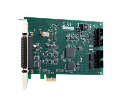
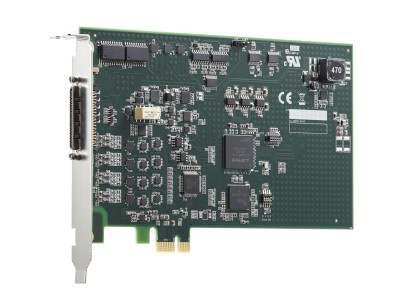
Comprehensive Product Summary: ADLINK DAQe‑2010 PCI Express Data Acquisition Card
*(Approx. 12 000 characters / ~3000 tokens)*
### 1. Product Overview
Product Name: DAQe‑2010
Article Number: DAQe‑2010
Series: DAQe‑2000 Series (PCI Express Simultaneous‑Sampling Multi‑Function DAQ Cards)
Model Type: PCI Express x1 lane data‑acquisition card
Manufacturer: ADLINK Technology Inc.
Form Factor: Half‑size PCI Express card (168 mm × 107 mm excluding connectors)
Interface Bus: PCI Express x1 (3.3 V or 5 V signaling compatible)
The DAQe‑2010 is the PCI Express variant of ADLINK’s high‑performance DAQ‑2000 family, providing four simultaneous 14‑bit analog input channels at up to 2 MS/s per channel. It integrates analog input, analog output, digital I/O, and timing functions on a single board for laboratory automation, ATE, and signal analysis applications.
### 2. Key Features
- High‑speed simultaneous sampling: 4 differential AI channels, 14‑bit resolution, 2 MS/s aggregate rate.
- Dual analog outputs: 2 × 12‑bit voltage outputs (±10 V or 0–10 V ranges) with 1 MS/s update rate and 2 k‑sample FIFO.
- Digital I/O: 24 TTL/CMOS‑compatible lines (8255 PIO architecture).
- Timer/Counter: 2 × 16‑bit general‑purpose up/down counters (40 MHz base clock, external up to 10 MHz).
- Triggering: software, external analog or digital, and SSI bus trigger sources with pre‑, post‑, middle‑, delay‑, and re‑trigger modes.
- Auto‑calibration: on‑board 5 V reference (±2 ppm/°C) with digital trim DACs for gain/offset correction.
- Scatter‑gather DMA: bus‑mastering DMA for high‑throughput data transfer without CPU intervention.
- Multiple‑card synchronization: System Synchronization Interface (SSI) for clock and trigger sharing among up to four cards.
- Comprehensive software support: Windows 7/8 x86/x64 and Linux drivers; SDKs for LabVIEW®, MATLAB®, C/C++, Visual Basic, and Visual Studio .NET.
- Compact design: low‑noise analog/digital segregation and half‑size PCB for space‑constrained systems.
### 3. Technical Specifications
Analog Input
- Channels: 4 simultaneous differential
- Resolution: 14 bits, no missing codes
- Max sampling rate: 2 MS/s aggregate (500 kS/s per channel typical continuous)
- Programmable gain: ×1, ×2, ×4, ×8
- Bipolar ranges: ±10 V, ±5 V, ±2.5 V, ±1.25 V
- Unipolar ranges: 0–10 V, 0–5 V, 0–2.5 V, 0–1.25 V
- Input coupling: DC
- Input impedance: 1 GΩ // 100 pF
- Over‑voltage protection: ±35 V continuous (power on), ±15 V (power off)
- CMRR (DC–60 Hz): ≈ 90 – 97 dB depending on range
- Small‑signal bandwidth (–3 dB): ≈ 1 MHz at gain 1
- FIFO buffer: 8 k samples
- Offset error (after cal): ±3 mV max
- Gain error (after cal): ±0.1 % FSR
- Data transfer: polling or scatter‑gather DMA
Analog Output
- Channels: 2 voltage outputs
- Resolution: 12 bits
- Output ranges: 0–10 V, ±10 V, 0–AOEXTREF, ±AOEXTREF
- Max update rate: 1 MS/s (1 µs interval)
- Slew rate: 20 V/µs
- Settling time: 3 µs to ±0.5 LSB
- Output impedance: ≈ 0.3 Ω
- Drive capacity: ±5 mA into ≤ 1500 pF load
- FIFO buffer: 2 k samples (1 k per channel)
- Offset error (after cal): ±3 mV
- Gain error (after cal): ±0.05 % of max output
- Protection: short‑circuit to ground
- Trigger sources: software, external analog/digital, SSI
- Trigger modes: post‑, delay‑, re‑trigger
Digital I/O
- 24 programmable TTL/CMOS lines (8255 PIO)
- Input Low ≤ 0.8 V, High ≥ 2.0 V
- Output Low ≤ 0.5 V @ 8 mA, High ≥ 2.7 V @ –0.4 mA
Timer/Counter
- 2 channels, 16‑bit resolution
- Clock sources: internal 40 MHz or external ≤ 10 MHz
- Modes: event counting, period/pulse‑width measurement, pulse generation (single, re‑triggered, continuous)
General & Environmental
- Dimensions: 168 mm × 107 mm (excl. connectors)
- Connector: 68‑pin VHDCI female
- Operating temperature: 0 – 55 °C
- Storage temperature: –20 – 70 °C
- Humidity: 5 – 95 % non‑condensing
- Power requirements (typical): +3.3 V @ 1.03 A, +12 V @ 0.75 A
- On‑board reference: +5 V ± 2 ppm/°C, 6 ppm/1000 h stability
### 4. Functionality and Applications
The DAQe‑2010 performs simultaneous analog input sampling across four differential channels to eliminate phase skew and common‑mode noise. Each channel is digitized by a dedicated 14‑bit ADC (LTC1414 or equivalent). Analog and digital triggering allow precise event‑based acquisition for transient capture, stimulus/response testing, and waveform generation. Typical uses include automotive sensor testing, biomedical signal measurement, process control, and ATE systems.
The card supports software‑controlled gain and range selection per channel, and can operate in single‑ended or differential modes. Analog outputs can generate arbitrary waveforms synchronously with inputs for closed‑loop testing. Digital I/O lines provide control and status interfacing to external equipment, while the timer/counters enable frequency measurement or pulse generation.
Multiple DAQe‑2010 cards can be synchronized through the SSI bus for expanded channel count and phase‑aligned sampling. The board is fully plug‑and‑play under PCI Express and requires no jumper configuration.
### 5. Components & Accessories
Included Items
- DAQe‑2010 PCIe card
- ADLINK All‑in‑One software CD with drivers and utilities
- Software installation guide
Optional Accessories
- DIN‑68S/1M: 68‑pin SCSI‑II termination board with DIN‑rail mount and 1 m ACL‑10568 cable.
- ACL‑10568‑1: 68‑pin VHDCI shielded cable.
- ACL‑SSI‑2/3/4: SSI bus cables for synchronizing 2, 3, or 4 devices.
Connectors and Pin Functions
Single 68‑pin VHDCI connector carries AI, AO, DIO, GPTC, trigger, and AFI signals. Key pins include CH0± to CH3± (analog inputs), DA0OUT/DA1OUT, AOEXTREF, EXTATRIG, EXTDTRIG, EXTWFTRG, AFI0/AFI1, and 24 digital I/O lines (PA0–PA7, PB0–PB7, PC0–PC7). A 20‑pin SSI header provides TIMEBASE, ADCONV, DAWR, SCAN_START, AD_TRIG, and DA_TRIG lines for multi‑card synchronization.
### 6. Installation & Setup
The DAQe‑2010 is a plug‑and‑play PCI Express device requiring no manual address or IRQ configuration. Installation steps:
1. Power off the PC and observe ESD precautions.
2. Insert the card into an available PCIe x1 slot.
3. Secure the bracket and connect the VHDCI cable to the termination board or custom fixture.
4. Install drivers from the ADLINK CD or website and verify operation using the AD‑Logger utility.
For multi‑card systems, link SSI connectors with ACL‑SSI cables and designate one card as master via software. External clock or trigger sources may be connected to EXTTIMEBASE, EXTATRIG, EXTDTRIG, or AFI pins as required.
### 7. Performance & Capabilities
- Analog Input Throughput: 2 MS/s aggregate (500 kS/s per channel typical continuous).
- Analog Output Speed: 1 MS/s per channel with 20 V/µs slew rate.
- FIFO Depths: AI 8 k samples; AO 2 k samples.
- DMA Bandwidth: bus‑master scatter‑gather DMA supports sustained multi‑MB/s transfer rates limited only by system memory and PCIe bandwidth.
- Accuracy: post‑calibration gain error ≤ 0.1 % FSR (AI) and ≤ 0.05 % (AO); offset ≤ ±3 mV.
- Noise Level: ≈ 0.6 LSBrms typical at ±10 V range.
- Trigger Latency: hardware trigger response < 1 µs.
- Synchronization: SSI bus supports TIMEBASE, ADCONV, DAWR, SCAN_START, AD_TRIG, DA_TRIG signals for phase‑aligned operation across cards.
Limitations: no built‑in isolation; input voltage must remain within ±35 V to avoid damage; maximum external clock frequency 40 MHz.
### 8. Standards & Compliance
- Bus Interface: PCI Express x1 compliant with PCIe Base Specification v1.1 and later.
- Electrical Levels: TTL/CMOS compatible digital I/O and trigger signals.
- Environmental: operating 0–55 °C, storage –20–70 °C, 5–95 % RH non‑condensing.
- Safety & EMC: designed to meet CE and FCC Class A requirements for industrial computers.
- PXI Compatibility: functional equivalent to PXI‑2010 for software and driver interchangeability.
### 9. Additional Information
Calibration and Maintenance
The board is factory‑calibrated and stores trim constants in EEPROM. Auto‑calibration can be invoked via software to compensate gain and offset drift without external equipment. Recommended warm‑up time is 15 minutes before calibration or precision measurement. Three user‑modifiable calibration banks allow storing constants for different environments.
Software Support
- Drivers & Libraries: D2K‑DASK for Windows NT/2000/XP/7/8; D2K‑DASK/X for Linux (kernel 2.4 and later).
- Programming Interfaces: DLL and header libraries for C/C++, Visual Basic, Delphi, Borland C++; ActiveX controls (D2K‑OCX); LabVIEW VIs (D2K‑LVIEW PnP); DAQBench ActiveX visualization suite.
- Utilities: AD‑Logger for data logging and configuration; PCI_SCAN for resource verification.
Warranty and Service
- Standard two‑year limited warranty (one year in China).
- Covers defects in materials and workmanship from shipment date.
- Excludes damage from misuse, improper storage, or unauthorized repair.
- RMA procedure available via ADLINK website (http://rma.adlinktech.com).
- Technical support: service@adlinktech.com | Tel +886‑2‑8226‑5877.
Maintenance Guidelines
Operate within specified temperature and humidity limits; avoid electrostatic discharge during handling; periodically run auto‑calibration to maintain accuracy. Firmware and driver updates are available from ADLINK’s support portal.
### Summary
The ADLINK DAQe‑2010 is a compact, high‑speed PCI Express data‑acquisition solution combining four simultaneous 14‑bit analog inputs, dual 12‑bit analog outputs, 24 digital I/O lines, and two 16‑bit timers on a single board. With 2 MS/s sampling, 1 MS/s output, auto‑calibration, and comprehensive triggering and synchronization features, it delivers laboratory‑grade performance for industrial and scientific applications requiring precise time‑aligned acquisition and generation. Extensive software support and driver compatibility ensure rapid integration into Windows or Linux measurement systems, making the DAQe‑2010 a versatile and cost‑effective choice for high‑speed multifunction DAQ tasks.


 SUCHEN SIE DIE PASSENDE
 05-06.pdf
PDF Catalog
05-06.pdf
PDF Catalog
 05-08.pdf
PDF Catalog
05-08.pdf
PDF Catalog
 DAQ-2000Series_Software_Support.pdf
PDF Catalog
DAQ-2000Series_Software_Support.pdf
PDF Catalog
 DAQe-2000_Series_Datasheet_en_20170808_v1.pdf
PDF Catalog
DAQe-2000_Series_Datasheet_en_20170808_v1.pdf
PDF Catalog
 DAQ-2000Series_Manual_5.pdf
Manual
DAQ-2000Series_Manual_5.pdf
Manual
 DAQ-2000Series_Manual_1.pdf
Manual
DAQ-2000Series_Manual_1.pdf
Manual