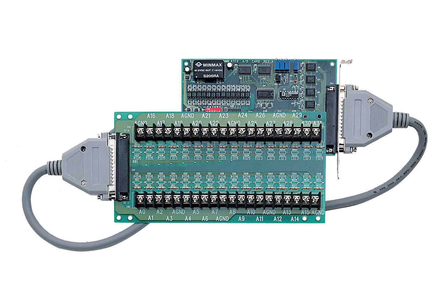
ACLD-9881
SUCHEN SIE DIE PASSENDE
INDUSTRIELLE LÖSUNG?
Entdecken Sie Embedded-, Kommunikations- und Automatisierungslösungen für Ihre Anwendung.
- PCI Bus Compatibility: Fully compliant with 32-bit PCI bus architecture; supports both 3.3 V and 5 V signaling environments.
- High-Speed Analog Input: 12-bit resolution with a maximum sampling rate of 110 kS/s and 8 µs conversion time.
- Flexible Input Configuration: 16 single-ended or 8 differential analog input channels.
- Programmable Gain Control: Software-selectable gains of ×0.5, ×1, ×2, ×4, and ×8 for optimal signal scaling.
- Wide Input Ranges: Bipolar (±0.625 V to ±10 V) and unipolar (0–1.25 V to 0–10 V) ranges.
- Automatic Channel Scanning: Hardware-supported auto-scan for sequential multi-channel sampling.
- Bus-Mastering DMA: High-speed, CPU-independent data transfer for analog input operations.
- Dual Analog Outputs: Two 12-bit multiplying DAC channels with programmable output ranges (0–5 V, 0–10 V, or external reference).
- Digital I/O: 16 TTL-compatible digital inputs and 16 TTL-compatible digital outputs.
- Timer/Counter: One 16-bit general-purpose counter/timer with a 2 MHz base clock and external clock capability up to 10 MHz.
- Overvoltage Protection: Continuous ±35 V protection on analog input channels.
- High Input Impedance: 1 GΩ input impedance ensures minimal signal loading.
- Integrated DC/DC Converter: Provides stable analog power for improved accuracy.
- Plug-and-Play Installation: Automatic resource allocation via PCI BIOS; no manual configuration required.
- Software Support: Compatible with Windows 7/8 (x86/x64) and Linux; drivers available for LabVIEW®, MATLAB®, C/C++, Visual Basic, and Visual Studio.NET.
- Utility Software: Includes AD-Logger for data logging and calibration utilities.
- High-Speed Analog Input: 12-bit resolution with a maximum sampling rate of 110 kS/s and 8 µs conversion time.
- Flexible Input Configuration: 16 single-ended or 8 differential analog input channels.
- Programmable Gain Control: Software-selectable gains of ×0.5, ×1, ×2, ×4, and ×8 for optimal signal scaling.
- Wide Input Ranges: Bipolar (±0.625 V to ±10 V) and unipolar (0–1.25 V to 0–10 V) ranges.
- Automatic Channel Scanning: Hardware-supported auto-scan for sequential multi-channel sampling.
- Bus-Mastering DMA: High-speed, CPU-independent data transfer for analog input operations.
- Dual Analog Outputs: Two 12-bit multiplying DAC channels with programmable output ranges (0–5 V, 0–10 V, or external reference).
- Digital I/O: 16 TTL-compatible digital inputs and 16 TTL-compatible digital outputs.
- Timer/Counter: One 16-bit general-purpose counter/timer with a 2 MHz base clock and external clock capability up to 10 MHz.
- Overvoltage Protection: Continuous ±35 V protection on analog input channels.
- High Input Impedance: 1 GΩ input impedance ensures minimal signal loading.
- Integrated DC/DC Converter: Provides stable analog power for improved accuracy.
- Plug-and-Play Installation: Automatic resource allocation via PCI BIOS; no manual configuration required.
- Software Support: Compatible with Windows 7/8 (x86/x64) and Linux; drivers available for LabVIEW®, MATLAB®, C/C++, Visual Basic, and Visual Studio.NET.
- Utility Software: Includes AD-Logger for data logging and calibration utilities.
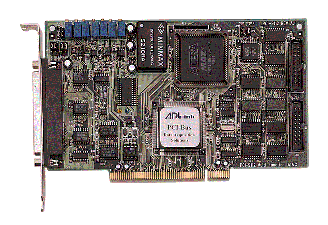
Comprehensive Product Summary: ADLINK PCI-9112A Multi-Function Data Acquisition Card
### 1. Product Overview
Product Name: PCI-9112A
Model: PCI-9112A
Series: NuDAQ® / NuIPC® 9112 Series
Article Number: PCI-9112A
Manufacturer: ADLINK Technology Inc.
Product Type: 16-Channel, 12-Bit, 110 kS/s Multi-Function PCI Data Acquisition (DAQ) Card
Calibration: Analog Output Calibrated on 10 V Reference
The ADLINK PCI-9112A is a high-performance, multi-function data acquisition card designed for PCI bus systems. It integrates analog input, analog output, digital I/O, and timing/counter functions into a single half-size PCI card. The PCI-9112A is part of ADLINK’s NuDAQ® 9112 series, which also includes the PCI-9112 (5 V calibration) and CompactPCI variants (cPCI-9112 and cPCI-9112R). The PCI-9112A is specifically calibrated for 10 V analog output operation, providing enhanced precision for industrial and laboratory measurement applications.
### 2. Key Features
- PCI Bus Compatibility: Fully compliant with 32-bit PCI bus architecture; supports both 3.3 V and 5 V signaling environments.
- High-Speed Analog Input: 12-bit resolution with a maximum sampling rate of 110 kS/s and 8 µs conversion time.
- Flexible Input Configuration: 16 single-ended or 8 differential analog input channels.
- Programmable Gain Control: Software-selectable gains of ×0.5, ×1, ×2, ×4, and ×8 for optimal signal scaling.
- Wide Input Ranges: Bipolar (±0.625 V to ±10 V) and unipolar (0–1.25 V to 0–10 V) ranges.
- Automatic Channel Scanning: Hardware-supported auto-scan for sequential multi-channel sampling.
- Bus-Mastering DMA: High-speed, CPU-independent data transfer for analog input operations.
- Dual Analog Outputs: Two 12-bit multiplying DAC channels with programmable output ranges (0–5 V, 0–10 V, or external reference).
- Digital I/O: 16 TTL-compatible digital inputs and 16 TTL-compatible digital outputs.
- Timer/Counter: One 16-bit general-purpose counter/timer with a 2 MHz base clock and external clock capability up to 10 MHz.
- Overvoltage Protection: Continuous ±35 V protection on analog input channels.
- High Input Impedance: 1 GΩ input impedance ensures minimal signal loading.
- Integrated DC/DC Converter: Provides stable analog power for improved accuracy.
- Plug-and-Play Installation: Automatic resource allocation via PCI BIOS; no manual configuration required.
- Software Support: Compatible with Windows 7/8 (x86/x64) and Linux; drivers available for LabVIEW®, MATLAB®, C/C++, Visual Basic, and Visual Studio.NET.
- Utility Software: Includes AD-Logger for data logging and calibration utilities.
### 3. Technical Specifications
Physical Characteristics
- Form Factor: Half-size PCI card
- Dimensions: 175 mm (L) × 107 mm (H) (6.82" × 4.17")
- Weight: Approx. 200 g (typical)
- PCB Material: Multi-layer FR-4 with gold-plated edge connector
Power Requirements
- +5 V @ 460 mA (typical)
- +12 V @ 110 mA (typical)
Environmental Conditions
- Operating Temperature: 0°C to 60°C (32°F to 140°F)
- Storage Temperature: –20°C to 80°C (–4°F to 176°F)
- Relative Humidity: 5% to 95%, non-condensing
### 4. Functionality
Analog Input (A/D Conversion)
- Channels: 16 single-ended or 8 differential
- Resolution: 12 bits
- Sampling Rate: Up to 110 kS/s
- Conversion Time: 8 µs per channel
- Input Ranges:
- Bipolar: ±10 V, ±5 V, ±2.5 V, ±1.25 V, ±0.625 V
- Unipolar: 0–10 V, 0–5 V, 0–2.5 V, 0–1.25 V
- Accuracy:
- Gain 0.5, 1: 0.01% of FSR ±1 LSB
- Gain 2, 4: 0.02% of FSR ±1 LSB
- Gain 8: 0.04% of FSR ±1 LSB
- Input Impedance: 1 GΩ (typical)
- Overvoltage Protection: ±35 V continuous
- Input Coupling: DC
- Trigger Modes: Software, Timer Pacer, External Trigger
- Data Transfer Modes: Programmed I/O, Interrupt, Bus-Mastering DMA
- FIFO Buffer: 1 k-sample hardware FIFO
Analog Output (D/A Conversion)
- Channels: 2 voltage outputs
- Resolution: 12 bits
- Output Ranges (software programmable):
- 0–5 V, 0–10 V, or 0–EXTREF (external reference)
- Output Drive Capability: ±5 mA maximum
- Settling Time: 30 µs to 0.5 LSB
- DAC Type: DAC7541 or equivalent multiplying DAC
- Calibration: PCI-9112A calibrated on 10 V reference
Digital I/O
- Channels: 16 inputs and 16 outputs
- Logic Level: 5 V TTL compatible
- Input Voltage:
- Logic Low: 0–0.8 V
- Logic High: ≥2.0 V
- Output Voltage:
- Logic Low: ≤0.4 V @ 8 mA sink
- Logic High: ≥2.4 V @ 0.4 mA source
- Data Transfer: Programmed I/O
Timer/Counter
- Device: Intel 8254-compatible
- Channels: 1 user-programmable 16-bit counter
- Base Clock: 2 MHz internal oscillator
- External Clock Input: Up to 10 MHz
- Modes: Programmable for event counting, frequency generation, or timing applications
### 5. Components & Accessories
Included Components:
- PCI-9112A DAQ card
- ADLINK Software CD (drivers, SDKs, utilities)
- Software Installation Guide
- User’s Manual
Optional Terminal Boards & Cables:
- DIN-37D-01: 37-pin D-sub terminal board with DIN-rail mounting
- DIN-20P-01: 20-pin ribbon connector terminal board
- ACLD-9137-01 / ACLD-9138-01: General-purpose terminal boards with 37-pin D-sub connectors
- ACLD-9182A-01 / ACLD-9185-01: 16-channel isolated digital input/output terminal boards
- ACL-10137-1MM / 1MF: 37-pin D-sub cables (male/male or male/female, 1 m)
- ACL-10120-1: 20-pin flat cable, 1 m
- ACL-10237-1: 37-pin flat cable, 1 m
Connectors:
- CN1: 20-pin digital input connector
- CN2: 20-pin digital output connector
- CN3: 37-pin D-sub analog I/O and timer/counter connector
### 6. Installation & Setup
System Requirements:
- PCI slot with bus-mastering capability
- Compatible operating systems: Windows 7/8 (x86/x64), Linux
- Minimum CPU: Pentium-class or higher
Installation Steps:
1. Power off the PC and remove the cover.
2. Insert the PCI-9112A into an available PCI slot.
3. Secure the card and reconnect system power.
4. Upon boot, the system BIOS automatically assigns resources (IRQ, I/O base).
5. Install drivers from the ADLINK Software CD.
6. Verify installation using the ADLINK utility (9112UTIL.EXE).
Jumper Configuration:
- JP1/JP5: Select single-ended or differential analog input mode.
- JP2: Select internal (2 MHz) or external clock source.
- JP3: Select D/A reference voltage (–5 V or –10 V).
- JP4: Select internal or external D/A reference source.
Calibration:
- PCI-9112A is factory-calibrated on 10 V reference.
- Onboard variable resistors (VR1–VR7) allow fine adjustment of A/D and D/A offsets and gains.
### 7. Performance & Capabilities
- A/D Throughput: 110 kS/s maximum
- A/D Conversion Time: 8 µs
- D/A Settling Time: 30 µs
- Timer Frequency Range: 0.00046 Hz to 100 kHz
- DMA Transfer Rate: Up to 32 million samples per session (bus-mastering mode)
- Accuracy: Up to 0.01% of full-scale range ±1 LSB (gain 1)
- Input Protection: ±35 V continuous
- Noise Rejection: High due to differential input option and 1 GΩ impedance
- Limitations:
- Single-ended mode susceptible to ground loops if improperly grounded
- Maximum sampling rate limited by PCI bus bandwidth and system latency
### 8. Standards & Compliance
- Bus Interface: PCI Local Bus Specification, Revision 2.2
- Electrical Compliance: 3.3 V / 5 V PCI signaling
- Safety & EMC: Designed to meet CE and FCC Class A requirements
- Environmental Compliance: RoHS-compliant manufacturing
- Software Standards:
- LabVIEW® VI support
- MATLAB® Data Acquisition Toolbox compatibility
- OPC, DDE, and ActiveX (DAQBench™) interfaces
- Industry Standards:
- IEEE 1057 (A/D converter performance)
- IEC 1131-3 (ISaGRAF™ SoftPLC compatibility)
### 9. Additional Information
Warranty:
- Two-year limited warranty (one year in China) from date of shipment.
- Covers manufacturing defects; excludes damage from misuse, environmental factors, or unauthorized repair.
Support & Service:
- Technical Support: automation@adlinktech.com
- Sales & Service: service@adlinktech.com
- Website: [www.adlinktech.com](http://www.adlinktech.com)
- Phone: +886-2-82265877
- Fax: +886-2-82265717
- Address: 9F, No. 166, Jian Yi Road, Chungho City, Taipei 235, Taiwan
Maintenance & Calibration:
- Recommended recalibration interval:
- Every 3 months for industrial environments
- Every 6–12 months for laboratory conditions
- Calibration utility included on software CD.
Software & SDKs:
- Drivers: PCIS-DASK for Windows 98/NT/2000/XP/7/8, Linux drivers available.
- Programming Libraries: C/C++, Visual Basic, Delphi, LabVIEW®, MATLAB®.
- Utilities:
- 9112UTIL.EXE for configuration, calibration, and functional testing
- PCI_SCAN.EXE for PCI device diagnostics
- AD-Logger for data acquisition and logging
Demo Programs:
- A/D, D/A, and DIO examples for DOS, C/C++, and Visual Basic environments.
- Demonstrations include software-triggered, interrupt-driven, and DMA-based data acquisition.
Applications:
- Industrial process control and monitoring
- Laboratory data logging and signal analysis
- Energy management and automation systems
- Product testing and quality assurance
- Event counting, waveform generation, and control systems
### Summary
The ADLINK PCI-9112A is a robust, high-precision, multi-function PCI data acquisition card engineered for demanding industrial and laboratory environments. With 12-bit resolution, 110 kS/s sampling rate, and versatile analog and digital I/O capabilities, it provides a comprehensive solution for measurement, control, and automation tasks. Its bus-mastering DMA, programmable gain, and dual 12-bit DAC outputs ensure efficient, accurate, and flexible data handling. Supported by extensive software tools and SDKs, the PCI-9112A integrates seamlessly into Windows and Linux systems, making it a reliable choice for engineers, researchers, and system integrators requiring precise and stable data acquisition performance.

### 1. Product Overview
Product Name: PCI-9112A
Model: PCI-9112A
Series: NuDAQ® / NuIPC® 9112 Series
Article Number: PCI-9112A
Manufacturer: ADLINK Technology Inc.
Product Type: 16-Channel, 12-Bit, 110 kS/s Multi-Function PCI Data Acquisition (DAQ) Card
Calibration: Analog Output Calibrated on 10 V Reference
The ADLINK PCI-9112A is a high-performance, multi-function data acquisition card designed for PCI bus systems. It integrates analog input, analog output, digital I/O, and timing/counter functions into a single half-size PCI card. The PCI-9112A is part of ADLINK’s NuDAQ® 9112 series, which also includes the PCI-9112 (5 V calibration) and CompactPCI variants (cPCI-9112 and cPCI-9112R). The PCI-9112A is specifically calibrated for 10 V analog output operation, providing enhanced precision for industrial and laboratory measurement applications.
### 2. Key Features
- PCI Bus Compatibility: Fully compliant with 32-bit PCI bus architecture; supports both 3.3 V and 5 V signaling environments.
- High-Speed Analog Input: 12-bit resolution with a maximum sampling rate of 110 kS/s and 8 µs conversion time.
- Flexible Input Configuration: 16 single-ended or 8 differential analog input channels.
- Programmable Gain Control: Software-selectable gains of ×0.5, ×1, ×2, ×4, and ×8 for optimal signal scaling.
- Wide Input Ranges: Bipolar (±0.625 V to ±10 V) and unipolar (0–1.25 V to 0–10 V) ranges.
- Automatic Channel Scanning: Hardware-supported auto-scan for sequential multi-channel sampling.
- Bus-Mastering DMA: High-speed, CPU-independent data transfer for analog input operations.
- Dual Analog Outputs: Two 12-bit multiplying DAC channels with programmable output ranges (0–5 V, 0–10 V, or external reference).
- Digital I/O: 16 TTL-compatible digital inputs and 16 TTL-compatible digital outputs.
- Timer/Counter: One 16-bit general-purpose counter/timer with a 2 MHz base clock and external clock capability up to 10 MHz.
- Overvoltage Protection: Continuous ±35 V protection on analog input channels.
- High Input Impedance: 1 GΩ input impedance ensures minimal signal loading.
- Integrated DC/DC Converter: Provides stable analog power for improved accuracy.
- Plug-and-Play Installation: Automatic resource allocation via PCI BIOS; no manual configuration required.
- Software Support: Compatible with Windows 7/8 (x86/x64) and Linux; drivers available for LabVIEW®, MATLAB®, C/C++, Visual Basic, and Visual Studio.NET.
- Utility Software: Includes AD-Logger for data logging and calibration utilities.
### 3. Technical Specifications
Physical Characteristics
- Form Factor: Half-size PCI card
- Dimensions: 175 mm (L) × 107 mm (H) (6.82" × 4.17")
- Weight: Approx. 200 g (typical)
- PCB Material: Multi-layer FR-4 with gold-plated edge connector
Power Requirements
- +5 V @ 460 mA (typical)
- +12 V @ 110 mA (typical)
Environmental Conditions
- Operating Temperature: 0°C to 60°C (32°F to 140°F)
- Storage Temperature: –20°C to 80°C (–4°F to 176°F)
- Relative Humidity: 5% to 95%, non-condensing
### 4. Functionality
Analog Input (A/D Conversion)
- Channels: 16 single-ended or 8 differential
- Resolution: 12 bits
- Sampling Rate: Up to 110 kS/s
- Conversion Time: 8 µs per channel
- Input Ranges:
- Bipolar: ±10 V, ±5 V, ±2.5 V, ±1.25 V, ±0.625 V
- Unipolar: 0–10 V, 0–5 V, 0–2.5 V, 0–1.25 V
- Accuracy:
- Gain 0.5, 1: 0.01% of FSR ±1 LSB
- Gain 2, 4: 0.02% of FSR ±1 LSB
- Gain 8: 0.04% of FSR ±1 LSB
- Input Impedance: 1 GΩ (typical)
- Overvoltage Protection: ±35 V continuous
- Input Coupling: DC
- Trigger Modes: Software, Timer Pacer, External Trigger
- Data Transfer Modes: Programmed I/O, Interrupt, Bus-Mastering DMA
- FIFO Buffer: 1 k-sample hardware FIFO
Analog Output (D/A Conversion)
- Channels: 2 voltage outputs
- Resolution: 12 bits
- Output Ranges (software programmable):
- 0–5 V, 0–10 V, or 0–EXTREF (external reference)
- Output Drive Capability: ±5 mA maximum
- Settling Time: 30 µs to 0.5 LSB
- DAC Type: DAC7541 or equivalent multiplying DAC
- Calibration: PCI-9112A calibrated on 10 V reference
Digital I/O
- Channels: 16 inputs and 16 outputs
- Logic Level: 5 V TTL compatible
- Input Voltage:
- Logic Low: 0–0.8 V
- Logic High: ≥2.0 V
- Output Voltage:
- Logic Low: ≤0.4 V @ 8 mA sink
- Logic High: ≥2.4 V @ 0.4 mA source
- Data Transfer: Programmed I/O
Timer/Counter
- Device: Intel 8254-compatible
- Channels: 1 user-programmable 16-bit counter
- Base Clock: 2 MHz internal oscillator
- External Clock Input: Up to 10 MHz
- Modes: Programmable for event counting, frequency generation, or timing applications
### 5. Components & Accessories
Included Components:
- PCI-9112A DAQ card
- ADLINK Software CD (drivers, SDKs, utilities)
- Software Installation Guide
- User’s Manual
Optional Terminal Boards & Cables:
- DIN-37D-01: 37-pin D-sub terminal board with DIN-rail mounting
- DIN-20P-01: 20-pin ribbon connector terminal board
- ACLD-9137-01 / ACLD-9138-01: General-purpose terminal boards with 37-pin D-sub connectors
- ACLD-9182A-01 / ACLD-9185-01: 16-channel isolated digital input/output terminal boards
- ACL-10137-1MM / 1MF: 37-pin D-sub cables (male/male or male/female, 1 m)
- ACL-10120-1: 20-pin flat cable, 1 m
- ACL-10237-1: 37-pin flat cable, 1 m
Connectors:
- CN1: 20-pin digital input connector
- CN2: 20-pin digital output connector
- CN3: 37-pin D-sub analog I/O and timer/counter connector
### 6. Installation & Setup
System Requirements:
- PCI slot with bus-mastering capability
- Compatible operating systems: Windows 7/8 (x86/x64), Linux
- Minimum CPU: Pentium-class or higher
Installation Steps:
1. Power off the PC and remove the cover.
2. Insert the PCI-9112A into an available PCI slot.
3. Secure the card and reconnect system power.
4. Upon boot, the system BIOS automatically assigns resources (IRQ, I/O base).
5. Install drivers from the ADLINK Software CD.
6. Verify installation using the ADLINK utility (9112UTIL.EXE).
Jumper Configuration:
- JP1/JP5: Select single-ended or differential analog input mode.
- JP2: Select internal (2 MHz) or external clock source.
- JP3: Select D/A reference voltage (–5 V or –10 V).
- JP4: Select internal or external D/A reference source.
Calibration:
- PCI-9112A is factory-calibrated on 10 V reference.
- Onboard variable resistors (VR1–VR7) allow fine adjustment of A/D and D/A offsets and gains.
### 7. Performance & Capabilities
- A/D Throughput: 110 kS/s maximum
- A/D Conversion Time: 8 µs
- D/A Settling Time: 30 µs
- Timer Frequency Range: 0.00046 Hz to 100 kHz
- DMA Transfer Rate: Up to 32 million samples per session (bus-mastering mode)
- Accuracy: Up to 0.01% of full-scale range ±1 LSB (gain 1)
- Input Protection: ±35 V continuous
- Noise Rejection: High due to differential input option and 1 GΩ impedance
- Limitations:
- Single-ended mode susceptible to ground loops if improperly grounded
- Maximum sampling rate limited by PCI bus bandwidth and system latency
### 8. Standards & Compliance
- Bus Interface: PCI Local Bus Specification, Revision 2.2
- Electrical Compliance: 3.3 V / 5 V PCI signaling
- Safety & EMC: Designed to meet CE and FCC Class A requirements
- Environmental Compliance: RoHS-compliant manufacturing
- Software Standards:
- LabVIEW® VI support
- MATLAB® Data Acquisition Toolbox compatibility
- OPC, DDE, and ActiveX (DAQBench™) interfaces
- Industry Standards:
- IEEE 1057 (A/D converter performance)
- IEC 1131-3 (ISaGRAF™ SoftPLC compatibility)
### 9. Additional Information
Warranty:
- Two-year limited warranty (one year in China) from date of shipment.
- Covers manufacturing defects; excludes damage from misuse, environmental factors, or unauthorized repair.
Support & Service:
- Technical Support: automation@adlinktech.com
- Sales & Service: service@adlinktech.com
- Website: [www.adlinktech.com](http://www.adlinktech.com)
- Phone: +886-2-82265877
- Fax: +886-2-82265717
- Address: 9F, No. 166, Jian Yi Road, Chungho City, Taipei 235, Taiwan
Maintenance & Calibration:
- Recommended recalibration interval:
- Every 3 months for industrial environments
- Every 6–12 months for laboratory conditions
- Calibration utility included on software CD.
Software & SDKs:
- Drivers: PCIS-DASK for Windows 98/NT/2000/XP/7/8, Linux drivers available.
- Programming Libraries: C/C++, Visual Basic, Delphi, LabVIEW®, MATLAB®.
- Utilities:
- 9112UTIL.EXE for configuration, calibration, and functional testing
- PCI_SCAN.EXE for PCI device diagnostics
- AD-Logger for data acquisition and logging
Demo Programs:
- A/D, D/A, and DIO examples for DOS, C/C++, and Visual Basic environments.
- Demonstrations include software-triggered, interrupt-driven, and DMA-based data acquisition.
Applications:
- Industrial process control and monitoring
- Laboratory data logging and signal analysis
- Energy management and automation systems
- Product testing and quality assurance
- Event counting, waveform generation, and control systems
### Summary
The ADLINK PCI-9112A is a robust, high-precision, multi-function PCI data acquisition card engineered for demanding industrial and laboratory environments. With 12-bit resolution, 110 kS/s sampling rate, and versatile analog and digital I/O capabilities, it provides a comprehensive solution for measurement, control, and automation tasks. Its bus-mastering DMA, programmable gain, and dual 12-bit DAC outputs ensure efficient, accurate, and flexible data handling. Supported by extensive software tools and SDKs, the PCI-9112A integrates seamlessly into Windows and Linux systems, making it a reliable choice for engineers, researchers, and system integrators requiring precise and stable data acquisition performance.
-
PCI-9112_Datasheet_en_2.pdf
PDF Catalog
-
PCI-9112_Manual_4.pdf
Manual
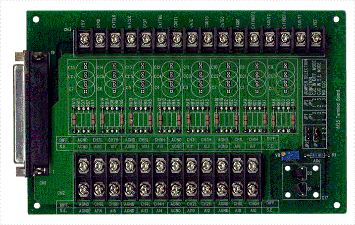
- ACLD-9881 - Panel for mounting low pass filter etc., incl. ACL-10137-1
- ACLD-8125 - Panel with cold junction compensation
- ACLD-9188 - Panel for mounting low pass filter etc.
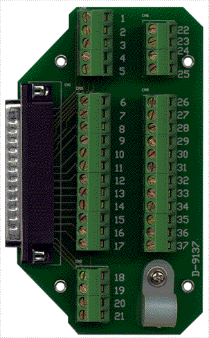
- ACLD-9137-01 - Direct 37 small screw terminal
- ACLD-9138-01 - Panel general purpose, 2*20 small screw terminal
- DIN-37D-01 - 37pin D-type panel DIN rail w/o cable
- ACL-10337 - 2*20 pin to DB 37 slot adapter