DIN-100S-01
SUCHEN SIE DIE PASSENDE
INDUSTRIELLE LÖSUNG?
Entdecken Sie Embedded-, Kommunikations- und Automatisierungslösungen für Ihre Anwendung.
- High-Speed PCI Express Interface:
PCIe x1 lane interface providing up to 80 MB/s sustained data transfer rate via bus mastering DMA.
- Flexible Channel Configuration:
32 channels of 5 V TTL-compatible digital I/O, configurable as 16 inputs and 16 outputs, or as 32 inputs or 32 outputs.
- High Throughput:
- Up to 80 MB/s sustained transfer rate (32-bit @ 20 MHz).
- Up to 160 MB/s burst rate for digital input using external 40 MHz clock.
- Large Onboard FIFO Buffers:
64 KB total FIFO memory (32 KB for input, 32 KB for output) for high-speed buffered data transfer.
- Advanced DMA Support:
Bus mastering DMA with scatter-gather capability for efficient, non-contiguous memory transfers and ring-buffer operation.
- Programmable Timing and Triggering:
- Onboard 8254 programmable timer/counter with 10 MHz base clock.
- Independent DI_TRG and DO_TRG trigger signals for acquisition and pattern generation.
- Internal or external clocking up to 40 MHz.
- Auxiliary I/O:
4 auxiliary digital inputs and 4 auxiliary digital outputs for control or status signaling.
- Active Termination:
Software-selectable active terminators for reliable high-speed and long-distance data transmission.
- Software and OS Support:
- Windows 7/Vista/XP/2000/2003 Server
- Linux (PCIS-DASK/X)
- Supported APIs: DAQPilot for LabVIEW™, PCIS-DASK, DAQBench, and AD-Logger.
- Programming languages: VB.NET, VC.NET, C/C++, Delphi, Borland C++ Builder.
- Plug and Play Configuration:
Fully compliant with PCI Plug and Play standards; no jumpers or DIP switches required.
PCIe x1 lane interface providing up to 80 MB/s sustained data transfer rate via bus mastering DMA.
- Flexible Channel Configuration:
32 channels of 5 V TTL-compatible digital I/O, configurable as 16 inputs and 16 outputs, or as 32 inputs or 32 outputs.
- High Throughput:
- Up to 80 MB/s sustained transfer rate (32-bit @ 20 MHz).
- Up to 160 MB/s burst rate for digital input using external 40 MHz clock.
- Large Onboard FIFO Buffers:
64 KB total FIFO memory (32 KB for input, 32 KB for output) for high-speed buffered data transfer.
- Advanced DMA Support:
Bus mastering DMA with scatter-gather capability for efficient, non-contiguous memory transfers and ring-buffer operation.
- Programmable Timing and Triggering:
- Onboard 8254 programmable timer/counter with 10 MHz base clock.
- Independent DI_TRG and DO_TRG trigger signals for acquisition and pattern generation.
- Internal or external clocking up to 40 MHz.
- Auxiliary I/O:
4 auxiliary digital inputs and 4 auxiliary digital outputs for control or status signaling.
- Active Termination:
Software-selectable active terminators for reliable high-speed and long-distance data transmission.
- Software and OS Support:
- Windows 7/Vista/XP/2000/2003 Server
- Linux (PCIS-DASK/X)
- Supported APIs: DAQPilot for LabVIEW™, PCIS-DASK, DAQBench, and AD-Logger.
- Programming languages: VB.NET, VC.NET, C/C++, Delphi, Borland C++ Builder.
- Plug and Play Configuration:
Fully compliant with PCI Plug and Play standards; no jumpers or DIP switches required.
Comprehensive Product Summary: ADLINK PCIe-7300A High-Speed Digital I/O Card
### 1. Product Overview
Product Name: PCIe-7300A
Model: PCIe-7300A
Series: PCI/PCIe-7300A, cPCI-7300 Series
Article Number: PCIe-7300A
Manufacturer: ADLINK Technology Inc.
Product Type: High-Speed 32-Channel Digital Input/Output (DIO) PCI Express Card
Form Factor: PCI Express x1 lane interface, 3U Eurocard (for cPCI variant)
Product Category: Data Acquisition and Digital I/O Interface Card
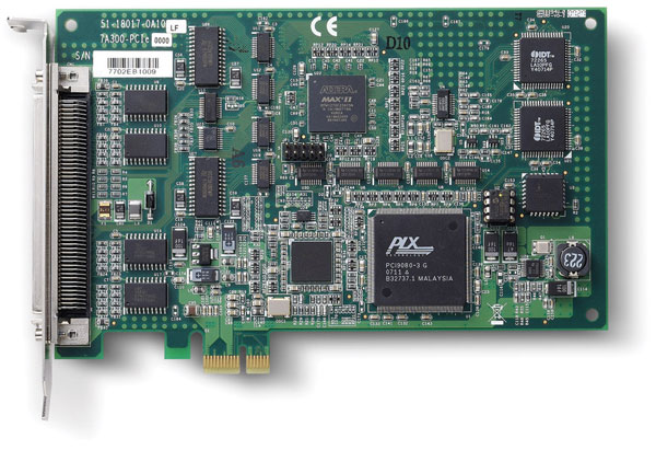
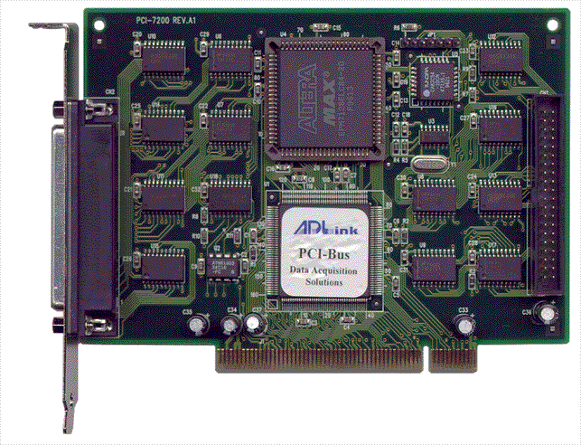
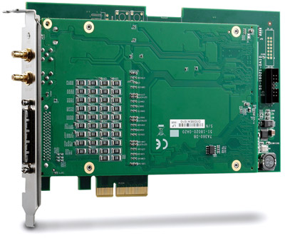
The ADLINK PCIe-7300A is a high-performance, bus-mastering digital I/O card designed for ultra-fast data acquisition, pattern generation, and digital signal interfacing. It belongs to ADLINK’s 7300 series, which includes PCI, PCIe, and CompactPCI (cPCI) variants, all engineered for high-speed digital I/O operations with advanced DMA and scatter-gather capabilities.
### 2. Key Features
- High-Speed PCI Express Interface:
PCIe x1 lane interface providing up to 80 MB/s sustained data transfer rate via bus mastering DMA.
- Flexible Channel Configuration:
32 channels of 5 V TTL-compatible digital I/O, configurable as 16 inputs and 16 outputs, or as 32 inputs or 32 outputs.
- High Throughput:
- Up to 80 MB/s sustained transfer rate (32-bit @ 20 MHz).
- Up to 160 MB/s burst rate for digital input using external 40 MHz clock.
- Large Onboard FIFO Buffers:
64 KB total FIFO memory (32 KB for input, 32 KB for output) for high-speed buffered data transfer.
- Advanced DMA Support:
Bus mastering DMA with scatter-gather capability for efficient, non-contiguous memory transfers and ring-buffer operation.
- Programmable Timing and Triggering:
- Onboard 8254 programmable timer/counter with 10 MHz base clock.
- Independent DI_TRG and DO_TRG trigger signals for acquisition and pattern generation.
- Internal or external clocking up to 40 MHz.
- Auxiliary I/O:
4 auxiliary digital inputs and 4 auxiliary digital outputs for control or status signaling.
- Active Termination:
Software-selectable active terminators for reliable high-speed and long-distance data transmission.
- Software and OS Support:
- Windows 7/Vista/XP/2000/2003 Server
- Linux (PCIS-DASK/X)
- Supported APIs: DAQPilot for LabVIEW™, PCIS-DASK, DAQBench, and AD-Logger.
- Programming languages: VB.NET, VC.NET, C/C++, Delphi, Borland C++ Builder.
- Plug and Play Configuration:
Fully compliant with PCI Plug and Play standards; no jumpers or DIP switches required.
### 3. Technical Specifications
Digital I/O Configuration:
- Channels: 32 total (software configurable as 16 DI/16 DO, 32 DI, or 32 DO)
- Logic Level: 5 V TTL compatible
- Input Voltage:
- High: 2.0 V to 5.25 V
- Low: 0 V to 0.8 V
- Output Voltage:
- High: ≥ 2.7 V
- Low: ≤ 0.5 V
- Output Drive Capability:
- Source: 8 mA
- Sink: 48 mA
Input Load Characteristics:
- Terminator OFF:
- Input high current: 1 mA
- Input low current: 20 mA
- Terminator ON:
- Termination resistor: 111 Ω
- Termination voltage: 2.9 V
- Input high current: 1 mA
- Input low current: 22.4 mA
Transfer Characteristics:
- Data Width: 8, 16, or 32 bits (programmable)
- Transfer Mode: Bus-mastering DMA with scatter/gather
- DMA Transfer Count:
- Non-chaining mode: 2M double words (8 MB)
- Chaining mode: Unlimited (scatter/gather)
Maximum Transfer Rates:
- Digital Output (DO): 80 MB/s (32-bit @ 20 MHz)
- Digital Input (DI): 80 MB/s (32-bit @ 20 MHz), up to 160 MB/s (32-bit @ 40 MHz external clock)
Trigger and Clocking:
- Trigger Inputs: DI_TRG, DO_TRG (5 V TTL)
- Trigger Edge: Rising or falling (programmable)
- Minimum Pulse Width: 32 ns
- Internal Clock Sources: 20 MHz, 10 MHz, Timer #0/#1 outputs
- External Clock: Up to 40 MHz
- Handshaking: REQ/ACK and burst handshaking supported
Programmable Counter (8254):
- Base Clock: 10 MHz
- Timer #0: Digital input pacer
- Timer #1: Digital output pacer
- Timer #2: Interrupt source
Environmental Conditions:
- Operating Temperature: 0°C to 60°C
- Storage Temperature: -20°C to 80°C
- Relative Humidity: 5% to 95%, non-condensing
Power Requirements:
- PCIe-7300A: +12 V @ 119 mA typical, +3.3 V @ 499 mA typical, +5 V @ 830 mA typical (terminator off)
- With terminator on: +5 V @ 1.0 A typical
Physical Dimensions:
- PCIe-7300A: 168 mm (L) × 112 mm (H)
- PCI-7300A: 179 mm × 106 mm
- cPCI-7300: 160 mm × 100 mm
Connector:
- One 100-pin SCSI-II female connector (AMP-787082-9 compatible)
### 4. Functionality
The PCIe-7300A provides high-speed digital I/O interfacing between a host computer and external digital devices. It supports multiple operation modes:
- Internal Clock Mode: Data transfer paced by onboard timer or fixed-frequency clock (10/20 MHz).
- External Clock Mode: Data transfer synchronized with external strobe signals (DI_REQ/DO_ACK).
- Handshaking Mode: REQ/ACK signaling ensures reliable data exchange without loss.
- Pattern Generation Mode: Repeated digital output patterns at programmable rates.
- Burst Handshaking Mode: Combines speed of clocked transfer with reliability of handshake.
Applications:
- High-speed data acquisition and digital pattern capture
- Automated test equipment (ATE)
- Logic analysis and digital waveform generation
- Parallel digital communication interfaces
- High-speed peripheral interfacing
- Real-time control and simulation systems
Compatibility:
- Compatible with 5 V TTL-level digital systems
- Supports external triggering and synchronization with other DAQ devices
### 5. Components & Accessories
Included Items:
- PCIe-7300A card
- Software and driver CD (DAQPilot, PCIS-DASK, DAQBench)
- User manual and installation guide
Optional Accessories:
- DIN-100S-01: Terminal board with one 100-pin SCSI-II connector, DIN-rail mountable.
- ACL-102100-1: 100-pin SCSI-II cable (1 meter, AMP-787082-9 compatible).
- ACL-10252-1: 100-pin to dual 50-pin cable (1 meter) for legacy DIN-502S replacement.
### 6. Installation & Setup
System Requirements:
- PCI Express slot (x1 or higher) supporting bus mastering
- Compatible operating system (Windows or Linux)
- Administrative privileges for driver installation
Installation Steps:
1. Power off the computer and disconnect peripherals.
2. Insert the PCIe-7300A into an available PCIe slot.
3. Secure the card and reconnect power.
4. Upon boot, the system BIOS automatically assigns resources (IRQ, I/O base address).
5. Install ADLINK drivers from the provided CD or download from ADLINK’s website.
6. Verify installation using the 7300AUTIL utility.
Connector Pinout:
- 100-pin SCSI-II connector includes 32 data lines (PA0–PA15, PB0–PB15), control lines (DI_REQ, DO_ACK, TRIG), auxiliary I/O, and ground references.
- TERMPWR pins provide 4.7 V for external terminators.
Termination:
- Software-selectable active terminators reduce signal reflection and noise for long cable runs.
### 7. Performance & Capabilities
- Data Throughput:
Sustained 80 MB/s via PCIe bus mastering DMA; up to 160 MB/s for short bursts (DI mode).
- FIFO Buffering:
Dual 16K-word FIFOs for input and output ensure continuous high-speed streaming.
- Timing Resolution:
50 ns timing resolution via onboard programmable counters.
- DMA Efficiency:
Scatter-gather DMA allows large, non-contiguous memory transfers without CPU overhead.
- Latency and Reliability:
Handshaking and trigger synchronization prevent data loss during high-speed operation.
- Limitations:
- External clock limited to 40 MHz.
- FIFO size limits maximum burst length to 16K samples.
- TTL-level only (no isolation).
### 8. Standards & Compliance
- Bus Interface Standards:
- PCI Express Base Specification compliant (x1 lane)
- CompactPCI compliant (PICMG 2.0 R2.1 for cPCI-7300)
- Electrical Standards:
- TTL logic level compatibility (5 V)
- Active termination for signal integrity
- Software & Driver Compliance:
- Windows and Linux driver certification (PCIS-DASK, DAQPilot)
- LabVIEW™ integration via DAQPilot
- Environmental & Safety:
- RoHS compliant
- CE and FCC Class A (industrial)
### 9. Additional Information
Warranty:
- 1-year limited warranty from date of purchase.
- Covers defects in materials and workmanship.
- Excludes damage from misuse, modification, or operation beyond specifications.
Support & Maintenance:
- Technical support via ADLINK website and authorized distributors.
- Firmware and driver updates available online.
- Replacement and repair services available under warranty terms.
Software Development Support:
- Comprehensive C/C++ and DLL libraries for Windows and DOS.
- Example programs and utilities for rapid application development.
- API functions for configuration, DMA control, pattern generation, and timer setup.
Documentation:
- Full user manual with register maps, timing diagrams, and programming references.
- Application notes for integration with LabVIEW, MATLAB, and custom software.
### Summary
The ADLINK PCIe-7300A is a robust, high-speed digital I/O solution engineered for demanding industrial and laboratory applications requiring precise timing, high throughput, and flexible digital interfacing. With its 32 TTL channels, 64 KB FIFO, 80 MB/s DMA throughput, and programmable timing features, it excels in automated testing, digital pattern generation, and high-speed data acquisition environments. Its PCI Express architecture ensures low-latency, high-bandwidth communication with the host system, while comprehensive software support simplifies integration into diverse development environments.
Ordering Information:
- PCIe-7300A: 80 MB/s High-Speed 32-CH Digital I/O PCIe Card
- PCI-7300A: 80 MB/s High-Speed 32-CH Digital I/O PCI Card
- cPCI-7300: 80 MB/s High-Speed 32-CH Digital I/O CompactPCI Module
Manufacturer Website: [www.adlinktech.com](https://www.adlinktech.com)
*(Approx. 12,000 characters / ~3,000 tokens)*

### 1. Product Overview
Product Name: PCIe-7300A
Model: PCIe-7300A
Series: PCI/PCIe-7300A, cPCI-7300 Series
Article Number: PCIe-7300A
Manufacturer: ADLINK Technology Inc.
Product Type: High-Speed 32-Channel Digital Input/Output (DIO) PCI Express Card
Form Factor: PCI Express x1 lane interface, 3U Eurocard (for cPCI variant)
Product Category: Data Acquisition and Digital I/O Interface Card
The ADLINK PCIe-7300A is a high-performance, bus-mastering digital I/O card designed for ultra-fast data acquisition, pattern generation, and digital signal interfacing. It belongs to ADLINK’s 7300 series, which includes PCI, PCIe, and CompactPCI (cPCI) variants, all engineered for high-speed digital I/O operations with advanced DMA and scatter-gather capabilities.
### 2. Key Features
- High-Speed PCI Express Interface:
PCIe x1 lane interface providing up to 80 MB/s sustained data transfer rate via bus mastering DMA.
- Flexible Channel Configuration:
32 channels of 5 V TTL-compatible digital I/O, configurable as 16 inputs and 16 outputs, or as 32 inputs or 32 outputs.
- High Throughput:
- Up to 80 MB/s sustained transfer rate (32-bit @ 20 MHz).
- Up to 160 MB/s burst rate for digital input using external 40 MHz clock.
- Large Onboard FIFO Buffers:
64 KB total FIFO memory (32 KB for input, 32 KB for output) for high-speed buffered data transfer.
- Advanced DMA Support:
Bus mastering DMA with scatter-gather capability for efficient, non-contiguous memory transfers and ring-buffer operation.
- Programmable Timing and Triggering:
- Onboard 8254 programmable timer/counter with 10 MHz base clock.
- Independent DI_TRG and DO_TRG trigger signals for acquisition and pattern generation.
- Internal or external clocking up to 40 MHz.
- Auxiliary I/O:
4 auxiliary digital inputs and 4 auxiliary digital outputs for control or status signaling.
- Active Termination:
Software-selectable active terminators for reliable high-speed and long-distance data transmission.
- Software and OS Support:
- Windows 7/Vista/XP/2000/2003 Server
- Linux (PCIS-DASK/X)
- Supported APIs: DAQPilot for LabVIEW™, PCIS-DASK, DAQBench, and AD-Logger.
- Programming languages: VB.NET, VC.NET, C/C++, Delphi, Borland C++ Builder.
- Plug and Play Configuration:
Fully compliant with PCI Plug and Play standards; no jumpers or DIP switches required.
### 3. Technical Specifications
Digital I/O Configuration:
- Channels: 32 total (software configurable as 16 DI/16 DO, 32 DI, or 32 DO)
- Logic Level: 5 V TTL compatible
- Input Voltage:
- High: 2.0 V to 5.25 V
- Low: 0 V to 0.8 V
- Output Voltage:
- High: ≥ 2.7 V
- Low: ≤ 0.5 V
- Output Drive Capability:
- Source: 8 mA
- Sink: 48 mA
Input Load Characteristics:
- Terminator OFF:
- Input high current: 1 mA
- Input low current: 20 mA
- Terminator ON:
- Termination resistor: 111 Ω
- Termination voltage: 2.9 V
- Input high current: 1 mA
- Input low current: 22.4 mA
Transfer Characteristics:
- Data Width: 8, 16, or 32 bits (programmable)
- Transfer Mode: Bus-mastering DMA with scatter/gather
- DMA Transfer Count:
- Non-chaining mode: 2M double words (8 MB)
- Chaining mode: Unlimited (scatter/gather)
Maximum Transfer Rates:
- Digital Output (DO): 80 MB/s (32-bit @ 20 MHz)
- Digital Input (DI): 80 MB/s (32-bit @ 20 MHz), up to 160 MB/s (32-bit @ 40 MHz external clock)
Trigger and Clocking:
- Trigger Inputs: DI_TRG, DO_TRG (5 V TTL)
- Trigger Edge: Rising or falling (programmable)
- Minimum Pulse Width: 32 ns
- Internal Clock Sources: 20 MHz, 10 MHz, Timer #0/#1 outputs
- External Clock: Up to 40 MHz
- Handshaking: REQ/ACK and burst handshaking supported
Programmable Counter (8254):
- Base Clock: 10 MHz
- Timer #0: Digital input pacer
- Timer #1: Digital output pacer
- Timer #2: Interrupt source
Environmental Conditions:
- Operating Temperature: 0°C to 60°C
- Storage Temperature: -20°C to 80°C
- Relative Humidity: 5% to 95%, non-condensing
Power Requirements:
- PCIe-7300A: +12 V @ 119 mA typical, +3.3 V @ 499 mA typical, +5 V @ 830 mA typical (terminator off)
- With terminator on: +5 V @ 1.0 A typical
Physical Dimensions:
- PCIe-7300A: 168 mm (L) × 112 mm (H)
- PCI-7300A: 179 mm × 106 mm
- cPCI-7300: 160 mm × 100 mm
Connector:
- One 100-pin SCSI-II female connector (AMP-787082-9 compatible)
### 4. Functionality
The PCIe-7300A provides high-speed digital I/O interfacing between a host computer and external digital devices. It supports multiple operation modes:
- Internal Clock Mode: Data transfer paced by onboard timer or fixed-frequency clock (10/20 MHz).
- External Clock Mode: Data transfer synchronized with external strobe signals (DI_REQ/DO_ACK).
- Handshaking Mode: REQ/ACK signaling ensures reliable data exchange without loss.
- Pattern Generation Mode: Repeated digital output patterns at programmable rates.
- Burst Handshaking Mode: Combines speed of clocked transfer with reliability of handshake.
Applications:
- High-speed data acquisition and digital pattern capture
- Automated test equipment (ATE)
- Logic analysis and digital waveform generation
- Parallel digital communication interfaces
- High-speed peripheral interfacing
- Real-time control and simulation systems
Compatibility:
- Compatible with 5 V TTL-level digital systems
- Supports external triggering and synchronization with other DAQ devices
### 5. Components & Accessories
Included Items:
- PCIe-7300A card
- Software and driver CD (DAQPilot, PCIS-DASK, DAQBench)
- User manual and installation guide
Optional Accessories:
- DIN-100S-01: Terminal board with one 100-pin SCSI-II connector, DIN-rail mountable.
- ACL-102100-1: 100-pin SCSI-II cable (1 meter, AMP-787082-9 compatible).
- ACL-10252-1: 100-pin to dual 50-pin cable (1 meter) for legacy DIN-502S replacement.
### 6. Installation & Setup
System Requirements:
- PCI Express slot (x1 or higher) supporting bus mastering
- Compatible operating system (Windows or Linux)
- Administrative privileges for driver installation
Installation Steps:
1. Power off the computer and disconnect peripherals.
2. Insert the PCIe-7300A into an available PCIe slot.
3. Secure the card and reconnect power.
4. Upon boot, the system BIOS automatically assigns resources (IRQ, I/O base address).
5. Install ADLINK drivers from the provided CD or download from ADLINK’s website.
6. Verify installation using the 7300AUTIL utility.
Connector Pinout:
- 100-pin SCSI-II connector includes 32 data lines (PA0–PA15, PB0–PB15), control lines (DI_REQ, DO_ACK, TRIG), auxiliary I/O, and ground references.
- TERMPWR pins provide 4.7 V for external terminators.
Termination:
- Software-selectable active terminators reduce signal reflection and noise for long cable runs.
### 7. Performance & Capabilities
- Data Throughput:
Sustained 80 MB/s via PCIe bus mastering DMA; up to 160 MB/s for short bursts (DI mode).
- FIFO Buffering:
Dual 16K-word FIFOs for input and output ensure continuous high-speed streaming.
- Timing Resolution:
50 ns timing resolution via onboard programmable counters.
- DMA Efficiency:
Scatter-gather DMA allows large, non-contiguous memory transfers without CPU overhead.
- Latency and Reliability:
Handshaking and trigger synchronization prevent data loss during high-speed operation.
- Limitations:
- External clock limited to 40 MHz.
- FIFO size limits maximum burst length to 16K samples.
- TTL-level only (no isolation).
### 8. Standards & Compliance
- Bus Interface Standards:
- PCI Express Base Specification compliant (x1 lane)
- CompactPCI compliant (PICMG 2.0 R2.1 for cPCI-7300)
- Electrical Standards:
- TTL logic level compatibility (5 V)
- Active termination for signal integrity
- Software & Driver Compliance:
- Windows and Linux driver certification (PCIS-DASK, DAQPilot)
- LabVIEW™ integration via DAQPilot
- Environmental & Safety:
- RoHS compliant
- CE and FCC Class A (industrial)
### 9. Additional Information
Warranty:
- 1-year limited warranty from date of purchase.
- Covers defects in materials and workmanship.
- Excludes damage from misuse, modification, or operation beyond specifications.
Support & Maintenance:
- Technical support via ADLINK website and authorized distributors.
- Firmware and driver updates available online.
- Replacement and repair services available under warranty terms.
Software Development Support:
- Comprehensive C/C++ and DLL libraries for Windows and DOS.
- Example programs and utilities for rapid application development.
- API functions for configuration, DMA control, pattern generation, and timer setup.
Documentation:
- Full user manual with register maps, timing diagrams, and programming references.
- Application notes for integration with LabVIEW, MATLAB, and custom software.
### Summary
The ADLINK PCIe-7300A is a robust, high-speed digital I/O solution engineered for demanding industrial and laboratory applications requiring precise timing, high throughput, and flexible digital interfacing. With its 32 TTL channels, 64 KB FIFO, 80 MB/s DMA throughput, and programmable timing features, it excels in automated testing, digital pattern generation, and high-speed data acquisition environments. Its PCI Express architecture ensures low-latency, high-bandwidth communication with the host system, while comprehensive software support simplifies integration into diverse development environments.
Ordering Information:
- PCIe-7300A: 80 MB/s High-Speed 32-CH Digital I/O PCIe Card
- PCI-7300A: 80 MB/s High-Speed 32-CH Digital I/O PCI Card
- cPCI-7300: 80 MB/s High-Speed 32-CH Digital I/O CompactPCI Module
Manufacturer Website: [www.adlinktech.com](https://www.adlinktech.com)
*(Approx. 12,000 characters / ~3,000 tokens)*
-
cPCI-7300_Datasheet_en_1.pdf
PDF Catalog
-
P7300A Manual.PDF
Manual
- DIN-100S-01 - 100pin SCSI-II termination board DIN rail w/o cable
- DIN-502S - 2*50pin SCSI-II termination board DIN rail