DIN-68S-01
LOOKING FOR THE RIGHT
INDUSTRIAL SOLUTION?
Discover embedded, communication and automation solutions tailored to your application.
- PCI Express Interface: x1 lane PCIe interface for high‑speed data throughput and plug‑and‑play configuration.
- High Channel Density: 96 single‑ended (SE) or 48 differential (DI) analog input channels; mixed‑mode operation supported.
- High Sampling Rate: Up to 3 MS/s maximum sampling rate (single‑channel).
- 12‑bit Resolution: No missing codes; precise A/D conversion for accurate signal representation.
- Programmable Gain: 10 selectable gains (×1, ×2, ×4, ×5, ×8, ×10, ×20, ×40, ×50, ×200).
- Wide Input Range: Bipolar ranges from ±0.05 V to ±10 V; unipolar ranges from 0–0.1 V to 0–10 V.
- Auto‑Calibration: Fully automatic calibration with onboard 5 V reference (±2 ppm/°C).
- FIFO Buffer: 1 k‑sample A/D FIFO for continuous high‑speed acquisition.
- Triggering: Software, external analog, external digital, and SSI (System Synchronization Interface) triggers.
- Trigger Modes: Pre‑trigger, post‑trigger, middle‑trigger, delay‑trigger, and repeated trigger.
- Scatter‑Gather DMA: High‑speed bus‑mastering DMA with scatter/gather support for efficient data transfer.
- Digital I/O: 24‑channel TTL‑compatible programmable I/O (8255 PIO).
- Synchronization: Multi‑card synchronization via SSI or PXI trigger bus.
- Software Support: Drivers and SDKs for Windows 7/8 (x86/x64) and Linux; compatible with LabVIEW®, MATLAB®, C/C++, Visual Basic, and Visual Studio .NET.
- Utility Software: AD‑Logger for data logging and monitoring.
- Compact Design: 168 mm × 107 mm PCB with dual 68‑pin VHDCI connectors.
- High Channel Density: 96 single‑ended (SE) or 48 differential (DI) analog input channels; mixed‑mode operation supported.
- High Sampling Rate: Up to 3 MS/s maximum sampling rate (single‑channel).
- 12‑bit Resolution: No missing codes; precise A/D conversion for accurate signal representation.
- Programmable Gain: 10 selectable gains (×1, ×2, ×4, ×5, ×8, ×10, ×20, ×40, ×50, ×200).
- Wide Input Range: Bipolar ranges from ±0.05 V to ±10 V; unipolar ranges from 0–0.1 V to 0–10 V.
- Auto‑Calibration: Fully automatic calibration with onboard 5 V reference (±2 ppm/°C).
- FIFO Buffer: 1 k‑sample A/D FIFO for continuous high‑speed acquisition.
- Triggering: Software, external analog, external digital, and SSI (System Synchronization Interface) triggers.
- Trigger Modes: Pre‑trigger, post‑trigger, middle‑trigger, delay‑trigger, and repeated trigger.
- Scatter‑Gather DMA: High‑speed bus‑mastering DMA with scatter/gather support for efficient data transfer.
- Digital I/O: 24‑channel TTL‑compatible programmable I/O (8255 PIO).
- Synchronization: Multi‑card synchronization via SSI or PXI trigger bus.
- Software Support: Drivers and SDKs for Windows 7/8 (x86/x64) and Linux; compatible with LabVIEW®, MATLAB®, C/C++, Visual Basic, and Visual Studio .NET.
- Utility Software: AD‑Logger for data logging and monitoring.
- Compact Design: 168 mm × 107 mm PCB with dual 68‑pin VHDCI connectors.
Comprehensive Product Summary: ADLINK DAQe‑2208 PCI Express Data Acquisition Card
### 1. Product Overview
Product Name: DAQe‑2208
Model Number: DAQe‑2208
Series: DAQ‑/DAQe‑/PXI‑2200 Series (High‑Performance Multi‑Function Data Acquisition Cards)
Article Number: DAQe‑2208
Manufacturer: ADLINK Technology Inc.
Product Type: PCI Express (x1 lane) Analog‑to‑Digital (A/D) Data Acquisition Card
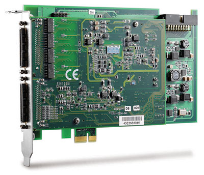
Product Description: 96‑channel, 12‑bit, 3 MS/s ultra‑high‑density analog input card with 1024‑word channel gain queue, 24‑channel digital I/O, and full auto‑calibration.
The DAQe‑2208 is part of ADLINK’s 2200‑series of high‑performance data acquisition (DAQ) cards designed for PCI Express systems. It provides high‑density analog input capability with flexible channel configuration, programmable gain, and multiple triggering and synchronization options. The card is optimized for high‑speed, high‑accuracy data logging, signal analysis, and automated test applications.
### 2. Key Features
- PCI Express Interface: x1 lane PCIe interface for high‑speed data throughput and plug‑and‑play configuration.
- High Channel Density: 96 single‑ended (SE) or 48 differential (DI) analog input channels; mixed‑mode operation supported.
- High Sampling Rate: Up to 3 MS/s maximum sampling rate (single‑channel).
- 12‑bit Resolution: No missing codes; precise A/D conversion for accurate signal representation.
- Programmable Gain: 10 selectable gains (×1, ×2, ×4, ×5, ×8, ×10, ×20, ×40, ×50, ×200).
- Wide Input Range: Bipolar ranges from ±0.05 V to ±10 V; unipolar ranges from 0–0.1 V to 0–10 V.
- Auto‑Calibration: Fully automatic calibration with onboard 5 V reference (±2 ppm/°C).
- FIFO Buffer: 1 k‑sample A/D FIFO for continuous high‑speed acquisition.
- Triggering: Software, external analog, external digital, and SSI (System Synchronization Interface) triggers.
- Trigger Modes: Pre‑trigger, post‑trigger, middle‑trigger, delay‑trigger, and repeated trigger.
- Scatter‑Gather DMA: High‑speed bus‑mastering DMA with scatter/gather support for efficient data transfer.
- Digital I/O: 24‑channel TTL‑compatible programmable I/O (8255 PIO).
- Synchronization: Multi‑card synchronization via SSI or PXI trigger bus.
- Software Support: Drivers and SDKs for Windows 7/8 (x86/x64) and Linux; compatible with LabVIEW®, MATLAB®, C/C++, Visual Basic, and Visual Studio .NET.
- Utility Software: AD‑Logger for data logging and monitoring.
- Compact Design: 168 mm × 107 mm PCB with dual 68‑pin VHDCI connectors.
### 3. Technical Specifications
Analog Input (AI):
- Channels: 96 SE or 48 DI (software‑selectable per channel).
- Resolution: 12 bits, no missing codes.
- Sampling Rate: Up to 3 MS/s (single‑channel).
- Input Coupling: DC.
- Input Impedance: 1 GΩ / 100 pF (power on).
- Overvoltage Protection: ±30 V (power on), ±15 V (power off).
- Input Range:
- *Bipolar:* ±10 V, ±5 V, ±2.5 V, ±2 V, ±1.25 V, ±1 V, ±0.5 V, ±0.25 V, ±0.2 V, ±0.05 V.
- *Unipolar:* 0–10 V, 0–5 V, 0–4 V, 0–2.5 V, 0–1 V, 0–0.5 V, 0–0.4 V, 0–0.1 V.
- Offset Error: ±2 mV typical.
- Gain Error: ±0.06 % of full‑scale range (FSR).
- Channel Gain Queue: 1024 configurations.
- FIFO Buffer: 1 k samples.
- Data Transfer: Polling or scatter‑gather DMA.
- CMRR: 90 dB typical (DC–60 Hz).
- Settling Time: 1 µs to 0.1 % error (typical).
Digital I/O (DIO):
- Channels: 24 TTL‑compatible programmable I/O (8255 PIO).
- Logic Levels:
- Input Low ≤ 0.8 V; Input High ≥ 2.0 V.
- Output Low ≤ 0.5 V @ 8 mA; Output High ≥ 2.7 V @ 400 µA.
- Transfer Mode: Programmed I/O.
Triggering:
- Sources: Software, external analog, external digital, SSI bus.
- Modes: Pre‑trigger, post‑trigger, middle‑trigger, delay‑trigger, repeated trigger.
- External Analog Trigger Input: ±10 V range, 8‑bit resolution, 400 kHz bandwidth.
- Digital Trigger: TTL/CMOS compatible, 10 ns minimum pulse width.
Synchronization:
- Interface: SSI (System Synchronization Interface) with 7 trigger lines.
- Functions: TIMEBASE, ADCONV, SCAN_START, AD_TRIG, DAWR, DA_TRIG.
- Multi‑Card Sync: Master/slave configuration via SSI or PXI trigger bus.
Physical & Electrical:
- Dimensions: 168 mm × 107 mm (excluding connectors).
- Connectors: Two 68‑pin VHDCI female connectors.
- Power Requirements (typical):
- +3.3 V @ 0.81 A
- +12 V @ 0.568 A
- Operating Temperature: 0 °C – 55 °C.
- Storage Temperature: −20 °C – 70 °C.
- Humidity: 5 % – 95 %, non‑condensing.
### 4. Functionality
Operation Principle:
The DAQe‑2208 converts analog signals into digital data via a 12‑bit A/D converter. Each channel can be configured independently for single‑ended or differential input. The onboard FIFO buffers data before transferring it to system memory through DMA. The card supports multiple trigger sources and modes, enabling precise control over acquisition timing.
Use Cases & Applications:
- Automated Test Equipment (ATE)
- Transient signal measurement
- Automotive and cable testing
- Laboratory automation and process control
- Biomedical and biotech instrumentation
- General‑purpose data logging and waveform analysis
Compatibility:
- Operating Systems: Windows 7/8 (x86/x64), Linux.
- Software Environments: LabVIEW®, MATLAB®, Visual Studio .NET, C/C++, Visual Basic.
- Drivers: D2K‑DASK (Windows), D2K‑DASK/X (Linux).
- Utilities: AD‑Logger for data recording and visualization.
### 5. Components & Accessories
Included Items:
- DAQe‑2208 PCIe data acquisition card.
- ADLINK All‑in‑One Software CD (drivers, SDKs, manuals).
- Software Installation Guide.
- User’s Manual (Rev. 2.01).
Optional Accessories:
- Terminal Boards:
- DIN‑68S‑01 (68‑pin screw terminal board).
- ACL‑10568‑1 (shielded cable assembly).
- Synchronization Cables:
- ACL‑SSI‑2/3/4 (SSI ribbon cables for multi‑card synchronization).
Connectors:
- Two 68‑pin VHDCI female connectors for analog and digital I/O.
- 20‑pin SSI connector for synchronization.
### 6. Installation & Setup
System Requirements:
- PCI Express slot (x1 or higher).
- Compatible operating system (Windows 7/8 or Linux).
- Administrative privileges for driver installation.
Installation Steps:
1. Power off the host PC and discharge static electricity.
2. Insert the DAQe‑2208 into an available PCIe slot.
3. Secure the card and reconnect power.
4. Install drivers from the ADLINK CD or website.
5. Verify installation using the PCI_SCAN utility.
Configuration:
- Plug‑and‑play PCIe configuration (no jumpers required).
- IRQ and base address automatically assigned by BIOS.
- Software‑configurable channel modes, gains, and ranges.
Mounting Options:
- Standard PCIe card mounting bracket.
- Compatible with standard PC chassis and industrial enclosures.
### 7. Performance & Capabilities
Analog Input Performance:
- Sampling Rate: 3 MS/s maximum (single‑channel).
- Resolution: 12 bits.
- Bandwidth: Up to 2 MHz small‑signal bandwidth (±10 V range).
- Noise: < 1 LSBrms typical.
- Settling Time: 1 µs to 0.1 % error.
- Gain Accuracy: ±0.03 % after calibration.
- Offset Accuracy: ±1 mV after calibration.
Data Transfer:
- DMA Mode: Bus‑mastering scatter/gather DMA for continuous high‑speed transfer.
- FIFO Buffer: 1 k samples (A/D).
Digital I/O Performance:
- Speed: TTL‑level I/O suitable for control and monitoring.
- Direction: Programmable per port (A, B, C).
Synchronization & Timing:
- Internal Clock: 40 MHz timebase.
- External Clock Input: 1 MHz – 40 MHz TTL.
- Trigger Latency: < 1 µs typical.
- Multi‑Card Sync: Deterministic timing via SSI bus.
Limitations:
- No analog output (D/A) or timer/counter functions on DAQe‑2208 (available on other 2200‑series models).
- Maximum sampling rate decreases in multi‑channel scanning mode.
### 8. Standards & Compliance
- Bus Interface: PCI Express® x1 lane compliant.
- PXI Compatibility: PXI Specification Rev. 2.2 (for PXI‑2208 variant).
- Electrical Standards: TTL/CMOS compatible digital I/O.
- Environmental: Operating 0 °C – 55 °C, 5 % – 95 % RH non‑condensing.
- Safety & EMC: Designed to meet CE and FCC Class A industrial standards.
- Calibration Reference: 5.000 V ± 2 ppm/°C onboard reference.
### 9. Additional Information
Calibration & Maintenance:
- Auto‑Calibration: Internal reference‑based automatic calibration; no external equipment required.
- User Calibration Storage: Up to three calibration sets stored in EEPROM with date and temperature.
- Recommended Warm‑Up: 15 minutes before calibration.
Warranty:
- Standard Warranty: Two years (one year in China).
- Coverage: Manufacturing defects; excludes misuse, environmental damage, or unauthorized repair.
- RMA Procedure: Submit RMA form via [rma.adlinktech.com/policy](http://rma.adlinktech.com/policy).
Technical Support:
- Global Offices:
- Taiwan (HQ): +886‑2‑8226‑5877, service@adlinktech.com
- USA: +1‑866‑4‑ADLINK, info@adlinktech.com
- Europe: +49‑211‑4955552, emea@adlinktech.com
- Singapore: +65‑6844‑2261, singapore@adlinktech.com
- China (Beijing/Shanghai/Shenzhen): market@adlinkchina.com.cn
Software & Driver Support:
- Windows Drivers: D2K‑DASK (DLL‑based API).
- Linux Drivers: D2K‑DASK/X (shared library).
- LabVIEW Integration: DAQ‑LVIEW PnP driver package.
- ActiveX Controls: D2K‑OCX for Visual Basic/VC++.
- Additional Tools: DAQBench ActiveX controls for GUI development.
Maintenance Recommendations:
- Handle using anti‑static precautions.
- Store in dry, temperature‑controlled environment (−20 °C – 70 °C).
- Periodically verify calibration for precision applications.
### Summary
The ADLINK DAQe‑2208 is a high‑density, high‑speed PCI Express data acquisition card engineered for demanding measurement and automation tasks. With 96 analog input channels, 12‑bit resolution, and a 3 MS/s sampling rate, it delivers exceptional performance for multi‑channel signal acquisition. Its flexible triggering, scatter‑gather DMA, and synchronization capabilities make it ideal for scalable, multi‑card systems. Full auto‑calibration, wide input ranges, and robust software support ensure reliable, precise, and easily integrated operation across industrial, laboratory, and research environments.

### 1. Product Overview
Product Name: DAQe‑2208
Model Number: DAQe‑2208
Series: DAQ‑/DAQe‑/PXI‑2200 Series (High‑Performance Multi‑Function Data Acquisition Cards)
Article Number: DAQe‑2208
Manufacturer: ADLINK Technology Inc.
Product Type: PCI Express (x1 lane) Analog‑to‑Digital (A/D) Data Acquisition Card
Product Description: 96‑channel, 12‑bit, 3 MS/s ultra‑high‑density analog input card with 1024‑word channel gain queue, 24‑channel digital I/O, and full auto‑calibration.
The DAQe‑2208 is part of ADLINK’s 2200‑series of high‑performance data acquisition (DAQ) cards designed for PCI Express systems. It provides high‑density analog input capability with flexible channel configuration, programmable gain, and multiple triggering and synchronization options. The card is optimized for high‑speed, high‑accuracy data logging, signal analysis, and automated test applications.
### 2. Key Features
- PCI Express Interface: x1 lane PCIe interface for high‑speed data throughput and plug‑and‑play configuration.
- High Channel Density: 96 single‑ended (SE) or 48 differential (DI) analog input channels; mixed‑mode operation supported.
- High Sampling Rate: Up to 3 MS/s maximum sampling rate (single‑channel).
- 12‑bit Resolution: No missing codes; precise A/D conversion for accurate signal representation.
- Programmable Gain: 10 selectable gains (×1, ×2, ×4, ×5, ×8, ×10, ×20, ×40, ×50, ×200).
- Wide Input Range: Bipolar ranges from ±0.05 V to ±10 V; unipolar ranges from 0–0.1 V to 0–10 V.
- Auto‑Calibration: Fully automatic calibration with onboard 5 V reference (±2 ppm/°C).
- FIFO Buffer: 1 k‑sample A/D FIFO for continuous high‑speed acquisition.
- Triggering: Software, external analog, external digital, and SSI (System Synchronization Interface) triggers.
- Trigger Modes: Pre‑trigger, post‑trigger, middle‑trigger, delay‑trigger, and repeated trigger.
- Scatter‑Gather DMA: High‑speed bus‑mastering DMA with scatter/gather support for efficient data transfer.
- Digital I/O: 24‑channel TTL‑compatible programmable I/O (8255 PIO).
- Synchronization: Multi‑card synchronization via SSI or PXI trigger bus.
- Software Support: Drivers and SDKs for Windows 7/8 (x86/x64) and Linux; compatible with LabVIEW®, MATLAB®, C/C++, Visual Basic, and Visual Studio .NET.
- Utility Software: AD‑Logger for data logging and monitoring.
- Compact Design: 168 mm × 107 mm PCB with dual 68‑pin VHDCI connectors.
### 3. Technical Specifications
Analog Input (AI):
- Channels: 96 SE or 48 DI (software‑selectable per channel).
- Resolution: 12 bits, no missing codes.
- Sampling Rate: Up to 3 MS/s (single‑channel).
- Input Coupling: DC.
- Input Impedance: 1 GΩ / 100 pF (power on).
- Overvoltage Protection: ±30 V (power on), ±15 V (power off).
- Input Range:
- *Bipolar:* ±10 V, ±5 V, ±2.5 V, ±2 V, ±1.25 V, ±1 V, ±0.5 V, ±0.25 V, ±0.2 V, ±0.05 V.
- *Unipolar:* 0–10 V, 0–5 V, 0–4 V, 0–2.5 V, 0–1 V, 0–0.5 V, 0–0.4 V, 0–0.1 V.
- Offset Error: ±2 mV typical.
- Gain Error: ±0.06 % of full‑scale range (FSR).
- Channel Gain Queue: 1024 configurations.
- FIFO Buffer: 1 k samples.
- Data Transfer: Polling or scatter‑gather DMA.
- CMRR: 90 dB typical (DC–60 Hz).
- Settling Time: 1 µs to 0.1 % error (typical).
Digital I/O (DIO):
- Channels: 24 TTL‑compatible programmable I/O (8255 PIO).
- Logic Levels:
- Input Low ≤ 0.8 V; Input High ≥ 2.0 V.
- Output Low ≤ 0.5 V @ 8 mA; Output High ≥ 2.7 V @ 400 µA.
- Transfer Mode: Programmed I/O.
Triggering:
- Sources: Software, external analog, external digital, SSI bus.
- Modes: Pre‑trigger, post‑trigger, middle‑trigger, delay‑trigger, repeated trigger.
- External Analog Trigger Input: ±10 V range, 8‑bit resolution, 400 kHz bandwidth.
- Digital Trigger: TTL/CMOS compatible, 10 ns minimum pulse width.
Synchronization:
- Interface: SSI (System Synchronization Interface) with 7 trigger lines.
- Functions: TIMEBASE, ADCONV, SCAN_START, AD_TRIG, DAWR, DA_TRIG.
- Multi‑Card Sync: Master/slave configuration via SSI or PXI trigger bus.
Physical & Electrical:
- Dimensions: 168 mm × 107 mm (excluding connectors).
- Connectors: Two 68‑pin VHDCI female connectors.
- Power Requirements (typical):
- +3.3 V @ 0.81 A
- +12 V @ 0.568 A
- Operating Temperature: 0 °C – 55 °C.
- Storage Temperature: −20 °C – 70 °C.
- Humidity: 5 % – 95 %, non‑condensing.
### 4. Functionality
Operation Principle:
The DAQe‑2208 converts analog signals into digital data via a 12‑bit A/D converter. Each channel can be configured independently for single‑ended or differential input. The onboard FIFO buffers data before transferring it to system memory through DMA. The card supports multiple trigger sources and modes, enabling precise control over acquisition timing.
Use Cases & Applications:
- Automated Test Equipment (ATE)
- Transient signal measurement
- Automotive and cable testing
- Laboratory automation and process control
- Biomedical and biotech instrumentation
- General‑purpose data logging and waveform analysis
Compatibility:
- Operating Systems: Windows 7/8 (x86/x64), Linux.
- Software Environments: LabVIEW®, MATLAB®, Visual Studio .NET, C/C++, Visual Basic.
- Drivers: D2K‑DASK (Windows), D2K‑DASK/X (Linux).
- Utilities: AD‑Logger for data recording and visualization.
### 5. Components & Accessories
Included Items:
- DAQe‑2208 PCIe data acquisition card.
- ADLINK All‑in‑One Software CD (drivers, SDKs, manuals).
- Software Installation Guide.
- User’s Manual (Rev. 2.01).
Optional Accessories:
- Terminal Boards:
- DIN‑68S‑01 (68‑pin screw terminal board).
- ACL‑10568‑1 (shielded cable assembly).
- Synchronization Cables:
- ACL‑SSI‑2/3/4 (SSI ribbon cables for multi‑card synchronization).
Connectors:
- Two 68‑pin VHDCI female connectors for analog and digital I/O.
- 20‑pin SSI connector for synchronization.
### 6. Installation & Setup
System Requirements:
- PCI Express slot (x1 or higher).
- Compatible operating system (Windows 7/8 or Linux).
- Administrative privileges for driver installation.
Installation Steps:
1. Power off the host PC and discharge static electricity.
2. Insert the DAQe‑2208 into an available PCIe slot.
3. Secure the card and reconnect power.
4. Install drivers from the ADLINK CD or website.
5. Verify installation using the PCI_SCAN utility.
Configuration:
- Plug‑and‑play PCIe configuration (no jumpers required).
- IRQ and base address automatically assigned by BIOS.
- Software‑configurable channel modes, gains, and ranges.
Mounting Options:
- Standard PCIe card mounting bracket.
- Compatible with standard PC chassis and industrial enclosures.
### 7. Performance & Capabilities
Analog Input Performance:
- Sampling Rate: 3 MS/s maximum (single‑channel).
- Resolution: 12 bits.
- Bandwidth: Up to 2 MHz small‑signal bandwidth (±10 V range).
- Noise: < 1 LSBrms typical.
- Settling Time: 1 µs to 0.1 % error.
- Gain Accuracy: ±0.03 % after calibration.
- Offset Accuracy: ±1 mV after calibration.
Data Transfer:
- DMA Mode: Bus‑mastering scatter/gather DMA for continuous high‑speed transfer.
- FIFO Buffer: 1 k samples (A/D).
Digital I/O Performance:
- Speed: TTL‑level I/O suitable for control and monitoring.
- Direction: Programmable per port (A, B, C).
Synchronization & Timing:
- Internal Clock: 40 MHz timebase.
- External Clock Input: 1 MHz – 40 MHz TTL.
- Trigger Latency: < 1 µs typical.
- Multi‑Card Sync: Deterministic timing via SSI bus.
Limitations:
- No analog output (D/A) or timer/counter functions on DAQe‑2208 (available on other 2200‑series models).
- Maximum sampling rate decreases in multi‑channel scanning mode.
### 8. Standards & Compliance
- Bus Interface: PCI Express® x1 lane compliant.
- PXI Compatibility: PXI Specification Rev. 2.2 (for PXI‑2208 variant).
- Electrical Standards: TTL/CMOS compatible digital I/O.
- Environmental: Operating 0 °C – 55 °C, 5 % – 95 % RH non‑condensing.
- Safety & EMC: Designed to meet CE and FCC Class A industrial standards.
- Calibration Reference: 5.000 V ± 2 ppm/°C onboard reference.
### 9. Additional Information
Calibration & Maintenance:
- Auto‑Calibration: Internal reference‑based automatic calibration; no external equipment required.
- User Calibration Storage: Up to three calibration sets stored in EEPROM with date and temperature.
- Recommended Warm‑Up: 15 minutes before calibration.
Warranty:
- Standard Warranty: Two years (one year in China).
- Coverage: Manufacturing defects; excludes misuse, environmental damage, or unauthorized repair.
- RMA Procedure: Submit RMA form via [rma.adlinktech.com/policy](http://rma.adlinktech.com/policy).
Technical Support:
- Global Offices:
- Taiwan (HQ): +886‑2‑8226‑5877, service@adlinktech.com
- USA: +1‑866‑4‑ADLINK, info@adlinktech.com
- Europe: +49‑211‑4955552, emea@adlinktech.com
- Singapore: +65‑6844‑2261, singapore@adlinktech.com
- China (Beijing/Shanghai/Shenzhen): market@adlinkchina.com.cn
Software & Driver Support:
- Windows Drivers: D2K‑DASK (DLL‑based API).
- Linux Drivers: D2K‑DASK/X (shared library).
- LabVIEW Integration: DAQ‑LVIEW PnP driver package.
- ActiveX Controls: D2K‑OCX for Visual Basic/VC++.
- Additional Tools: DAQBench ActiveX controls for GUI development.
Maintenance Recommendations:
- Handle using anti‑static precautions.
- Store in dry, temperature‑controlled environment (−20 °C – 70 °C).
- Periodically verify calibration for precision applications.
### Summary
The ADLINK DAQe‑2208 is a high‑density, high‑speed PCI Express data acquisition card engineered for demanding measurement and automation tasks. With 96 analog input channels, 12‑bit resolution, and a 3 MS/s sampling rate, it delivers exceptional performance for multi‑channel signal acquisition. Its flexible triggering, scatter‑gather DMA, and synchronization capabilities make it ideal for scalable, multi‑card systems. Full auto‑calibration, wide input ranges, and robust software support ensure reliable, precise, and easily integrated operation across industrial, laboratory, and research environments.
-
DAQ_DAQe_PXI-2208_Datasheet_en_2.pdf
PDF Catalog

- DIN-68S-01 - 68pin SCSI-II termination board DIN rail w/o cable
- ACL-10568-1 - SCSI-VHDCI cable 1m for DAQ series
- ACL-10568-2 - SCSI-VHDCI cable 2m for DAQ series
- ACL-10568-3 - SCSI-VHDCI cable 3m for DAQ series