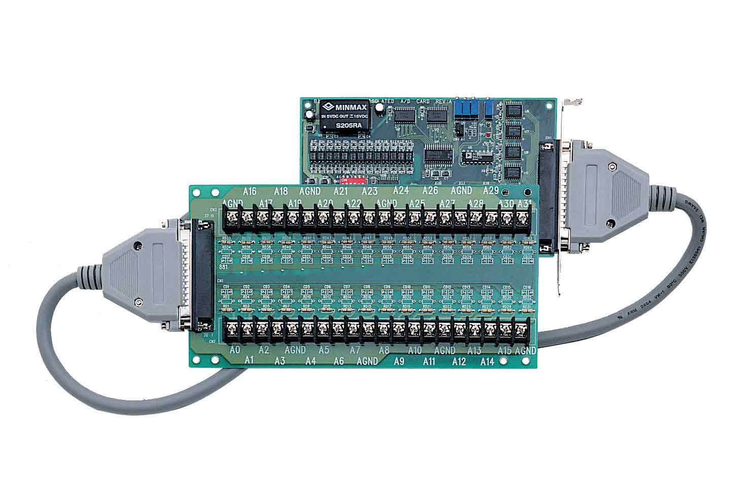
ACLD-9881
LOOKING FOR THE RIGHT
INDUSTRIAL SOLUTION?
Discover embedded, communication and automation solutions tailored to your application.
- High-Speed Analog Input:
16 single-ended or 8 differential analog input channels with 12-bit resolution and up to 110 kS/s sampling rate.
- Flexible Input Ranges:
Programmable bipolar and unipolar ranges:
- Bipolar: ±10 V, ±5 V, ±2.5 V, ±1.25 V, ±0.625 V
- Unipolar: 0–10 V, 0–5 V, 0–2.5 V, 0–1.25 V
- Programmable Gain Amplifier:
Software-selectable gains of ×0.5, ×1, ×2, ×4, ×8 for optimized signal conditioning.
- Analog Output:
Two 12-bit D/A channels (DAC7541 or equivalent) with software-programmable ranges (0–5 V, 0–10 V, or external reference up to ±10 V).
Output drive: ±5 mA, settling time: 30 µs to 0.5 LSB.
- Digital I/O:
16 TTL-compatible digital inputs and 16 TTL-compatible digital outputs for control and monitoring.
- Timer/Counter:
One 16-bit general-purpose counter (8254 device) with 2 MHz base clock, external clock up to 10 MHz.
- Bus-Mastering DMA:
High-speed data transfer via PCI bus mastering DMA for efficient analog input acquisition.
- Auto-Scan Function:
Automatic channel scanning for sequential analog input sampling.
- Trigger Modes:
Software, timer pacer, and external trigger modes for flexible acquisition control.
- Operating System Support:
Windows 7/8 (x86/x64) and Linux.
- Software & SDK Support:
Compatible with LabVIEW®, MATLAB®, Visual Studio®, C/C++, and Visual Basic.
Includes AD-Logger utility and PCIS-DASK driver library.
- Calibration Options:
- PCI-9112: Analog Output calibrated on 5 V reference
- PCI-9112A: Analog Output calibrated on 10 V reference
- Plug-and-Play PCI Configuration:
Fully compliant with PCI 2.1 specification, automatic resource allocation (IRQ, I/O base address).
16 single-ended or 8 differential analog input channels with 12-bit resolution and up to 110 kS/s sampling rate.
- Flexible Input Ranges:
Programmable bipolar and unipolar ranges:
- Bipolar: ±10 V, ±5 V, ±2.5 V, ±1.25 V, ±0.625 V
- Unipolar: 0–10 V, 0–5 V, 0–2.5 V, 0–1.25 V
- Programmable Gain Amplifier:
Software-selectable gains of ×0.5, ×1, ×2, ×4, ×8 for optimized signal conditioning.
- Analog Output:
Two 12-bit D/A channels (DAC7541 or equivalent) with software-programmable ranges (0–5 V, 0–10 V, or external reference up to ±10 V).
Output drive: ±5 mA, settling time: 30 µs to 0.5 LSB.
- Digital I/O:
16 TTL-compatible digital inputs and 16 TTL-compatible digital outputs for control and monitoring.
- Timer/Counter:
One 16-bit general-purpose counter (8254 device) with 2 MHz base clock, external clock up to 10 MHz.
- Bus-Mastering DMA:
High-speed data transfer via PCI bus mastering DMA for efficient analog input acquisition.
- Auto-Scan Function:
Automatic channel scanning for sequential analog input sampling.
- Trigger Modes:
Software, timer pacer, and external trigger modes for flexible acquisition control.
- Operating System Support:
Windows 7/8 (x86/x64) and Linux.
- Software & SDK Support:
Compatible with LabVIEW®, MATLAB®, Visual Studio®, C/C++, and Visual Basic.
Includes AD-Logger utility and PCIS-DASK driver library.
- Calibration Options:
- PCI-9112: Analog Output calibrated on 5 V reference
- PCI-9112A: Analog Output calibrated on 10 V reference
- Plug-and-Play PCI Configuration:
Fully compliant with PCI 2.1 specification, automatic resource allocation (IRQ, I/O base address).
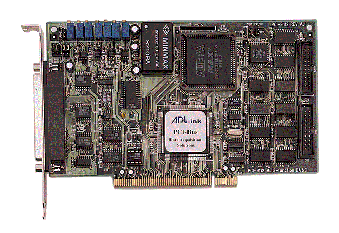
Comprehensive Product Summary: ADLINK PCI-9112 Multi-Function Data Acquisition Card
### 1. Product Overview
Product Name: PCI-9112
Model: PCI-9112 / PCI-9112A
Series: NuDAQ® / NuIPC® 9112 Series
Article Number: PCI-9112
Manufacturer: ADLINK Technology Inc.
Product Type: 16-Channel, 12-Bit, 110 kS/s Multi-Function Data Acquisition (DAQ) Card
Form Factor: PCI (32-bit, 3.3 V / 5 V compatible)
The ADLINK PCI-9112 is a high-performance, multi-function data acquisition card designed for industrial, laboratory, and embedded measurement applications. It integrates analog input, analog output, digital I/O, and timer/counter functions into a single PCI-based board, providing a cost-effective and flexible solution for data logging, process control, and signal analysis.
### 2. Key Features
- High-Speed Analog Input:
16 single-ended or 8 differential analog input channels with 12-bit resolution and up to 110 kS/s sampling rate.
- Flexible Input Ranges:
Programmable bipolar and unipolar ranges:
- Bipolar: ±10 V, ±5 V, ±2.5 V, ±1.25 V, ±0.625 V
- Unipolar: 0–10 V, 0–5 V, 0–2.5 V, 0–1.25 V
- Programmable Gain Amplifier:
Software-selectable gains of ×0.5, ×1, ×2, ×4, ×8 for optimized signal conditioning.
- Analog Output:
Two 12-bit D/A channels (DAC7541 or equivalent) with software-programmable ranges (0–5 V, 0–10 V, or external reference up to ±10 V).
Output drive: ±5 mA, settling time: 30 µs to 0.5 LSB.
- Digital I/O:
16 TTL-compatible digital inputs and 16 TTL-compatible digital outputs for control and monitoring.
- Timer/Counter:
One 16-bit general-purpose counter (8254 device) with 2 MHz base clock, external clock up to 10 MHz.
- Bus-Mastering DMA:
High-speed data transfer via PCI bus mastering DMA for efficient analog input acquisition.
- Auto-Scan Function:
Automatic channel scanning for sequential analog input sampling.
- Trigger Modes:
Software, timer pacer, and external trigger modes for flexible acquisition control.
- Operating System Support:
Windows 7/8 (x86/x64) and Linux.
- Software & SDK Support:
Compatible with LabVIEW®, MATLAB®, Visual Studio®, C/C++, and Visual Basic.
Includes AD-Logger utility and PCIS-DASK driver library.
- Calibration Options:
- PCI-9112: Analog Output calibrated on 5 V reference
- PCI-9112A: Analog Output calibrated on 10 V reference
- Plug-and-Play PCI Configuration:
Fully compliant with PCI 2.1 specification, automatic resource allocation (IRQ, I/O base address).
### 3. Technical Specifications
Analog Input (A/D):
- Channels: 16 single-ended or 8 differential
- Resolution: 12 bits
- Converter Type: Successive approximation (ADS774 or equivalent)
- Sampling Rate: Up to 110 kS/s
- Conversion Time: 8 µs
- Input Impedance: 10 MΩ
- Input Coupling: DC
- Overvoltage Protection: ±35 V continuous
- Accuracy:
- Gain 0.5, 1: 0.01% of FSR ±1 LSB
- Gain 2, 4: 0.02% of FSR ±1 LSB
- Gain 8: 0.04% of FSR ±1 LSB
- FIFO Buffer: 1 k-sample (PCI-9112)
- Trigger Modes: Software, Timer Pacer, External
- Data Transfer: Programmed I/O, Interrupt, Bus-Mastering DMA
Analog Output (D/A):
- Channels: 2
- Resolution: 12 bits
- Output Ranges: 0–5 V, 0–10 V, or 0–EXTREF (software programmable)
- Output Drive: ±5 mA
- Settling Time: 30 µs to 0.5 LSB
- Converter: DAC7541 or equivalent
- Data Transfer: Programmed I/O
Digital I/O:
- Inputs: 16 channels (TTL-compatible)
- Outputs: 16 channels (TTL-compatible)
- Input Voltage: Low ≤ 0.8 V, High ≥ 2.0 V
- Output Voltage: Low ≤ 0.4 V, High ≥ 2.4 V
- Drive Capability: Sink 8 mA, Source 0.4 mA
Timer/Counter:
- Device: 8254 programmable counter
- Channels: 1 user counter + 2 cascaded for A/D pacer
- Resolution: 16 bits
- Base Clock: 2 MHz internal oscillator
- External Clock Input: up to 10 MHz
- Pacer Frequency Range: 0.00046 Hz to 100 kHz
Physical & Environmental:
- Dimensions: 175 mm × 107 mm (6.89" × 4.21")
- Operating Temperature: 0°C to 60°C
- Storage Temperature: -20°C to 80°C
- Humidity: 5%–95% RH, non-condensing
- Power Requirements:
- +5 V @ 460 mA typical
- +12 V @ 110 mA typical
- Connector: 37-pin D-sub female (analog I/O), two 20-pin headers (digital I/O)
### 4. Functionality
The PCI-9112 performs simultaneous analog and digital data acquisition and control. It converts analog signals into digital data for processing and can generate analog output signals for control or simulation.
Use Cases & Applications:
- Industrial process monitoring and control
- Laboratory data logging and analysis
- Energy management systems
- Product testing and quality assurance
- Event counting and frequency measurement
- Waveform and pulse generation
- Security and annunciation systems
Compatibility:
- PCI bus (32-bit, 3.3 V/5 V signaling)
- Compatible with ADLINK terminal boards and cables
- Supported by ADLINK’s PCIS-DASK driver and SDK for Windows and Linux
### 5. Components & Accessories
Included:
- PCI-9112 or PCI-9112A DAQ card
- ADLINK Software CD (drivers, utilities, SDKs)
- Software Installation Guide
- User Manual
Optional Terminal Boards & Cables:
- DIN-37D-01: 37-pin D-sub terminal board with DIN-rail mount
- DIN-20P-01: 20-pin ribbon terminal board with DIN-rail mount
- ACLD-9137-01 / ACLD-9138-01: General-purpose terminal boards
- ACLD-9182A-01 / ACLD-9185-01: 16-channel isolated digital input/output boards
- ACL-10137-1MM / 1MF: 37-pin D-sub cables (male/male or male/female, 1 m)
- ACL-10120-1: 20-pin flat cable (1 m)
- ACL-10237-1: 37-pin flat cable (1 m)
### 6. Installation & Setup
Requirements:
- Available PCI slot with bus-mastering capability
- Compatible operating system (Windows 7/8 or Linux)
- Administrator privileges for driver installation
Installation Steps:
1. Power off the PC and disconnect peripherals.
2. Insert the PCI-9112 into an available PCI slot.
3. Secure the card and reconnect system power.
4. Upon boot, Windows Plug-and-Play detects the card automatically.
5. Install drivers from the ADLINK Software CD.
6. Verify installation using the AD-Logger or 9112 Utility software.
Jumper Configuration:
- JP1/JP5: Select single-ended or differential input mode
- JP2: Select internal (2 MHz) or external clock source
- JP3: Set D/A reference voltage (-5 V or -10 V)
- JP4: Select internal or external D/A reference source
Connectors:
- CN1: 20-pin digital input header
- CN2: 20-pin digital output header
- CN3: 37-pin D-sub for analog I/O and counter/timer signals
### 7. Performance & Capabilities
- A/D Throughput: 110 kS/s maximum
- A/D Accuracy: Up to 0.01% of FSR ±1 LSB
- D/A Settling Time: 30 µs
- DMA Transfer Rate: High-speed PCI bus mastering for continuous acquisition
- Timer Resolution: 0.5 µs (2 MHz base clock)
- FIFO Buffer: 1 k-sample for analog input
- Latency: Minimal due to direct memory access (DMA)
- Limitations:
- Single-ended mode limited to 16 channels
- Differential mode limited to 8 channels
- Analog output unipolar only (0–5 V or 0–10 V)
### 8. Standards & Compliance
- Bus Interface: PCI Local Bus Specification Rev. 2.1 compliant
- Electrical Compatibility: 3.3 V / 5 V PCI signaling
- Safety & Environmental:
- CE compliant
- RoHS compliant
- Software Standards:
- Compatible with NI LabVIEW®, MATLAB®, and OPC standards
- Supports ActiveX, DDE, and ISaGRAF™ interfaces
### 9. Additional Information
Calibration:
- Factory-calibrated prior to shipment
- Onboard variable resistors (VR1–VR7) for A/D and D/A fine-tuning
- Software calibration utility included for periodic recalibration
- Recommended recalibration interval:
- 3 months (industrial environments)
- 6–12 months (laboratory environments)
Maintenance:
- Handle in anti-static conditions
- Avoid exposure to high humidity or temperature extremes
- Use ADLINK calibration utility for accuracy verification
Warranty & Support:
- Standard 2-year limited warranty (1 year in China)
- Covers manufacturing defects and hardware failures
- Excludes damage from misuse, improper installation, or environmental factors
- Technical support via:
- Email: service@adlinktech.com
- Web: [www.adlinktech.com](http://www.adlinktech.com)
- Phone: +886-2-82265877
Software Utilities:
- 9112UTIL.EXE: Configuration, calibration, and functional testing utility
- PCI_SCAN.EXE: PCI device diagnostic tool
- Demo Programs:
- AD_DEMO1–6: A/D acquisition examples (software, interrupt, DMA modes)
- DA_DEMO: D/A output demonstration
- DIO_DEMO: Digital I/O control example
Driver & SDK Packages:
- PCIS-DASK: Windows driver and DLL library
- PCIS-LVIEW: LabVIEW® driver
- PCIS-VEE: HP-VEE driver
- DAQBench™: ActiveX control library
- PCIS-OPC: OPC server for industrial integration
### Summary
The ADLINK PCI-9112 is a robust, multi-function PCI data acquisition card offering 12-bit resolution, 110 kS/s sampling, and comprehensive analog and digital I/O capabilities. Its combination of high-speed A/D conversion, dual D/A outputs, programmable gain, and flexible triggering makes it ideal for a wide range of measurement and control applications. With full software support, plug-and-play PCI configuration, and optional terminal accessories, the PCI-9112 provides a complete, scalable solution for engineers and system integrators seeking reliable and precise data acquisition performance.

### 1. Product Overview
Product Name: PCI-9112
Model: PCI-9112 / PCI-9112A
Series: NuDAQ® / NuIPC® 9112 Series
Article Number: PCI-9112
Manufacturer: ADLINK Technology Inc.
Product Type: 16-Channel, 12-Bit, 110 kS/s Multi-Function Data Acquisition (DAQ) Card
Form Factor: PCI (32-bit, 3.3 V / 5 V compatible)
The ADLINK PCI-9112 is a high-performance, multi-function data acquisition card designed for industrial, laboratory, and embedded measurement applications. It integrates analog input, analog output, digital I/O, and timer/counter functions into a single PCI-based board, providing a cost-effective and flexible solution for data logging, process control, and signal analysis.
### 2. Key Features
- High-Speed Analog Input:
16 single-ended or 8 differential analog input channels with 12-bit resolution and up to 110 kS/s sampling rate.
- Flexible Input Ranges:
Programmable bipolar and unipolar ranges:
- Bipolar: ±10 V, ±5 V, ±2.5 V, ±1.25 V, ±0.625 V
- Unipolar: 0–10 V, 0–5 V, 0–2.5 V, 0–1.25 V
- Programmable Gain Amplifier:
Software-selectable gains of ×0.5, ×1, ×2, ×4, ×8 for optimized signal conditioning.
- Analog Output:
Two 12-bit D/A channels (DAC7541 or equivalent) with software-programmable ranges (0–5 V, 0–10 V, or external reference up to ±10 V).
Output drive: ±5 mA, settling time: 30 µs to 0.5 LSB.
- Digital I/O:
16 TTL-compatible digital inputs and 16 TTL-compatible digital outputs for control and monitoring.
- Timer/Counter:
One 16-bit general-purpose counter (8254 device) with 2 MHz base clock, external clock up to 10 MHz.
- Bus-Mastering DMA:
High-speed data transfer via PCI bus mastering DMA for efficient analog input acquisition.
- Auto-Scan Function:
Automatic channel scanning for sequential analog input sampling.
- Trigger Modes:
Software, timer pacer, and external trigger modes for flexible acquisition control.
- Operating System Support:
Windows 7/8 (x86/x64) and Linux.
- Software & SDK Support:
Compatible with LabVIEW®, MATLAB®, Visual Studio®, C/C++, and Visual Basic.
Includes AD-Logger utility and PCIS-DASK driver library.
- Calibration Options:
- PCI-9112: Analog Output calibrated on 5 V reference
- PCI-9112A: Analog Output calibrated on 10 V reference
- Plug-and-Play PCI Configuration:
Fully compliant with PCI 2.1 specification, automatic resource allocation (IRQ, I/O base address).
### 3. Technical Specifications
Analog Input (A/D):
- Channels: 16 single-ended or 8 differential
- Resolution: 12 bits
- Converter Type: Successive approximation (ADS774 or equivalent)
- Sampling Rate: Up to 110 kS/s
- Conversion Time: 8 µs
- Input Impedance: 10 MΩ
- Input Coupling: DC
- Overvoltage Protection: ±35 V continuous
- Accuracy:
- Gain 0.5, 1: 0.01% of FSR ±1 LSB
- Gain 2, 4: 0.02% of FSR ±1 LSB
- Gain 8: 0.04% of FSR ±1 LSB
- FIFO Buffer: 1 k-sample (PCI-9112)
- Trigger Modes: Software, Timer Pacer, External
- Data Transfer: Programmed I/O, Interrupt, Bus-Mastering DMA
Analog Output (D/A):
- Channels: 2
- Resolution: 12 bits
- Output Ranges: 0–5 V, 0–10 V, or 0–EXTREF (software programmable)
- Output Drive: ±5 mA
- Settling Time: 30 µs to 0.5 LSB
- Converter: DAC7541 or equivalent
- Data Transfer: Programmed I/O
Digital I/O:
- Inputs: 16 channels (TTL-compatible)
- Outputs: 16 channels (TTL-compatible)
- Input Voltage: Low ≤ 0.8 V, High ≥ 2.0 V
- Output Voltage: Low ≤ 0.4 V, High ≥ 2.4 V
- Drive Capability: Sink 8 mA, Source 0.4 mA
Timer/Counter:
- Device: 8254 programmable counter
- Channels: 1 user counter + 2 cascaded for A/D pacer
- Resolution: 16 bits
- Base Clock: 2 MHz internal oscillator
- External Clock Input: up to 10 MHz
- Pacer Frequency Range: 0.00046 Hz to 100 kHz
Physical & Environmental:
- Dimensions: 175 mm × 107 mm (6.89" × 4.21")
- Operating Temperature: 0°C to 60°C
- Storage Temperature: -20°C to 80°C
- Humidity: 5%–95% RH, non-condensing
- Power Requirements:
- +5 V @ 460 mA typical
- +12 V @ 110 mA typical
- Connector: 37-pin D-sub female (analog I/O), two 20-pin headers (digital I/O)
### 4. Functionality
The PCI-9112 performs simultaneous analog and digital data acquisition and control. It converts analog signals into digital data for processing and can generate analog output signals for control or simulation.
Use Cases & Applications:
- Industrial process monitoring and control
- Laboratory data logging and analysis
- Energy management systems
- Product testing and quality assurance
- Event counting and frequency measurement
- Waveform and pulse generation
- Security and annunciation systems
Compatibility:
- PCI bus (32-bit, 3.3 V/5 V signaling)
- Compatible with ADLINK terminal boards and cables
- Supported by ADLINK’s PCIS-DASK driver and SDK for Windows and Linux
### 5. Components & Accessories
Included:
- PCI-9112 or PCI-9112A DAQ card
- ADLINK Software CD (drivers, utilities, SDKs)
- Software Installation Guide
- User Manual
Optional Terminal Boards & Cables:
- DIN-37D-01: 37-pin D-sub terminal board with DIN-rail mount
- DIN-20P-01: 20-pin ribbon terminal board with DIN-rail mount
- ACLD-9137-01 / ACLD-9138-01: General-purpose terminal boards
- ACLD-9182A-01 / ACLD-9185-01: 16-channel isolated digital input/output boards
- ACL-10137-1MM / 1MF: 37-pin D-sub cables (male/male or male/female, 1 m)
- ACL-10120-1: 20-pin flat cable (1 m)
- ACL-10237-1: 37-pin flat cable (1 m)
### 6. Installation & Setup
Requirements:
- Available PCI slot with bus-mastering capability
- Compatible operating system (Windows 7/8 or Linux)
- Administrator privileges for driver installation
Installation Steps:
1. Power off the PC and disconnect peripherals.
2. Insert the PCI-9112 into an available PCI slot.
3. Secure the card and reconnect system power.
4. Upon boot, Windows Plug-and-Play detects the card automatically.
5. Install drivers from the ADLINK Software CD.
6. Verify installation using the AD-Logger or 9112 Utility software.
Jumper Configuration:
- JP1/JP5: Select single-ended or differential input mode
- JP2: Select internal (2 MHz) or external clock source
- JP3: Set D/A reference voltage (-5 V or -10 V)
- JP4: Select internal or external D/A reference source
Connectors:
- CN1: 20-pin digital input header
- CN2: 20-pin digital output header
- CN3: 37-pin D-sub for analog I/O and counter/timer signals
### 7. Performance & Capabilities
- A/D Throughput: 110 kS/s maximum
- A/D Accuracy: Up to 0.01% of FSR ±1 LSB
- D/A Settling Time: 30 µs
- DMA Transfer Rate: High-speed PCI bus mastering for continuous acquisition
- Timer Resolution: 0.5 µs (2 MHz base clock)
- FIFO Buffer: 1 k-sample for analog input
- Latency: Minimal due to direct memory access (DMA)
- Limitations:
- Single-ended mode limited to 16 channels
- Differential mode limited to 8 channels
- Analog output unipolar only (0–5 V or 0–10 V)
### 8. Standards & Compliance
- Bus Interface: PCI Local Bus Specification Rev. 2.1 compliant
- Electrical Compatibility: 3.3 V / 5 V PCI signaling
- Safety & Environmental:
- CE compliant
- RoHS compliant
- Software Standards:
- Compatible with NI LabVIEW®, MATLAB®, and OPC standards
- Supports ActiveX, DDE, and ISaGRAF™ interfaces
### 9. Additional Information
Calibration:
- Factory-calibrated prior to shipment
- Onboard variable resistors (VR1–VR7) for A/D and D/A fine-tuning
- Software calibration utility included for periodic recalibration
- Recommended recalibration interval:
- 3 months (industrial environments)
- 6–12 months (laboratory environments)
Maintenance:
- Handle in anti-static conditions
- Avoid exposure to high humidity or temperature extremes
- Use ADLINK calibration utility for accuracy verification
Warranty & Support:
- Standard 2-year limited warranty (1 year in China)
- Covers manufacturing defects and hardware failures
- Excludes damage from misuse, improper installation, or environmental factors
- Technical support via:
- Email: service@adlinktech.com
- Web: [www.adlinktech.com](http://www.adlinktech.com)
- Phone: +886-2-82265877
Software Utilities:
- 9112UTIL.EXE: Configuration, calibration, and functional testing utility
- PCI_SCAN.EXE: PCI device diagnostic tool
- Demo Programs:
- AD_DEMO1–6: A/D acquisition examples (software, interrupt, DMA modes)
- DA_DEMO: D/A output demonstration
- DIO_DEMO: Digital I/O control example
Driver & SDK Packages:
- PCIS-DASK: Windows driver and DLL library
- PCIS-LVIEW: LabVIEW® driver
- PCIS-VEE: HP-VEE driver
- DAQBench™: ActiveX control library
- PCIS-OPC: OPC server for industrial integration
### Summary
The ADLINK PCI-9112 is a robust, multi-function PCI data acquisition card offering 12-bit resolution, 110 kS/s sampling, and comprehensive analog and digital I/O capabilities. Its combination of high-speed A/D conversion, dual D/A outputs, programmable gain, and flexible triggering makes it ideal for a wide range of measurement and control applications. With full software support, plug-and-play PCI configuration, and optional terminal accessories, the PCI-9112 provides a complete, scalable solution for engineers and system integrators seeking reliable and precise data acquisition performance.
-
PCI-9112_Datasheet_en_2.pdf
PDF Catalog
-
PCI-9112_Manual_4.pdf
Manual
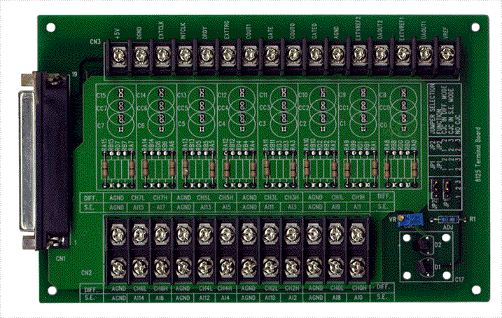
- ACLD-9881 - Panel for mounting low pass filter etc., incl. ACL-10137-1
- ACLD-8125 - Panel with cold junction compensation
- ACLD-9188 - Panel for mounting low pass filter etc.
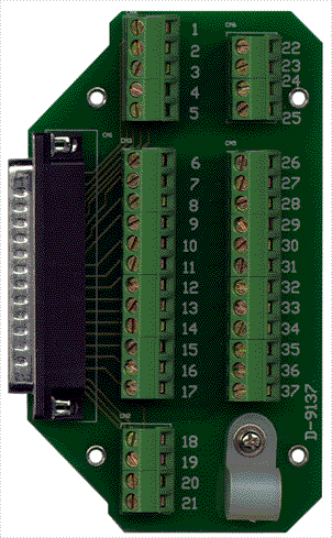
- ACLD-9137-01 - Direct 37 small screw terminal
- ACLD-9138-01 - Panel general purpose, 2*20 small screw terminal
- DIN-37D-01 - 37pin D-type panel DIN rail w/o cable
- ACL-10337 - 2*20 pin to DB 37 slot adapter