ACLD-8125
SUCHEN SIE DIE PASSENDE
INDUSTRIELLE LÖSUNG?
Entdecken Sie Embedded-, Kommunikations- und Automatisierungslösungen für Ihre Anwendung.
- High‑Resolution Analog Input: 16‑bit successive approximation A/D converter (ADS7805 or equivalent).
- Flexible Channel Configuration: 16 single‑ended or 8 differential analog input channels.
- Programmable Input Range: Bipolar ±10 V, ±5 V, ±2.5 V, ±1.25 V.
- Programmable Gain: ×1, ×2, ×4, ×8.
- High Sampling Rate: Up to 100 kHz for single‑channel, 20 kHz for multi‑channel multiplexed operation.
- Fast Conversion: 8 µs conversion time.
- Dual 12‑bit D/A Outputs: Two double‑buffered analog output channels (DAC7541 or equivalent).
- Selectable Output Range: 0–5 V or 0–10 V (internal reference), ±10 V (external reference).
- Digital I/O: 16 TTL‑compatible inputs and 16 TTL‑compatible outputs.
- Programmable Counter/Timer: Three 16‑bit counters (Intel 8254) with 2 MHz base clock.
- Trigger Modes: Software, programmable pacer (timer), or external pulse trigger.
- Data Transfer Options: Polling, interrupt, or DMA (channels 1 or 3).
- Interrupt Support: Selectable IRQ3, 5, 6, 7, 9, 10, 11, 12, or 15.
- Integrated DC/DC Converter: Provides stable analog power isolation.
- Compact Design: Half‑size ISA card (163 mm × 123 mm).
- Connectors: One 37‑pin D‑type and two 20‑pin IDC connectors.
- Software Support: DOS C/C++ library, Windows DLL (ACLS‑DLL2), and LabVIEW driver (ACLS‑LVIEW).
- Calibration Support: On‑board variable resistors (VRs) for A/D and D/A calibration.
- Flexible Channel Configuration: 16 single‑ended or 8 differential analog input channels.
- Programmable Input Range: Bipolar ±10 V, ±5 V, ±2.5 V, ±1.25 V.
- Programmable Gain: ×1, ×2, ×4, ×8.
- High Sampling Rate: Up to 100 kHz for single‑channel, 20 kHz for multi‑channel multiplexed operation.
- Fast Conversion: 8 µs conversion time.
- Dual 12‑bit D/A Outputs: Two double‑buffered analog output channels (DAC7541 or equivalent).
- Selectable Output Range: 0–5 V or 0–10 V (internal reference), ±10 V (external reference).
- Digital I/O: 16 TTL‑compatible inputs and 16 TTL‑compatible outputs.
- Programmable Counter/Timer: Three 16‑bit counters (Intel 8254) with 2 MHz base clock.
- Trigger Modes: Software, programmable pacer (timer), or external pulse trigger.
- Data Transfer Options: Polling, interrupt, or DMA (channels 1 or 3).
- Interrupt Support: Selectable IRQ3, 5, 6, 7, 9, 10, 11, 12, or 15.
- Integrated DC/DC Converter: Provides stable analog power isolation.
- Compact Design: Half‑size ISA card (163 mm × 123 mm).
- Connectors: One 37‑pin D‑type and two 20‑pin IDC connectors.
- Software Support: DOS C/C++ library, Windows DLL (ACLS‑DLL2), and LabVIEW driver (ACLS‑LVIEW).
- Calibration Support: On‑board variable resistors (VRs) for A/D and D/A calibration.
Comprehensive Product Summary – ADLINK ACL‑8216 High‑Resolution Multi‑Function Data Acquisition Card
### 1. Product Overview
Product Name: ACL‑8216
Model: ACL‑8216
Series: NuDAQ ISA‑Bus Data Acquisition Series
Article Number: ACL‑8216
Manufacturer: ADLINK Technology Inc.
Manufacturer Address: 9F, No. 166, Jian Yi Road, Chungho City, Taipei 235, Taiwan, R.O.C.
Website: [www.adlink.com.tw](http://www.adlink.com.tw)
Support Contacts:
- Sales & Service: service@adlink.com.tw
- Technical Support (NuDAQ): nudaq@adlink.com.tw
- Software Support: sw@adlink.com.tw
- Telephone: +886‑2‑82265877
- Fax: +886‑2‑82265717
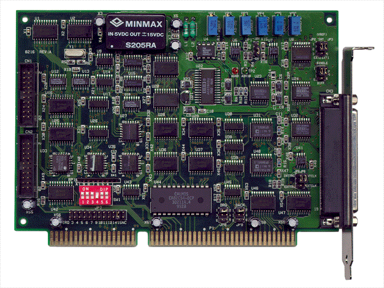
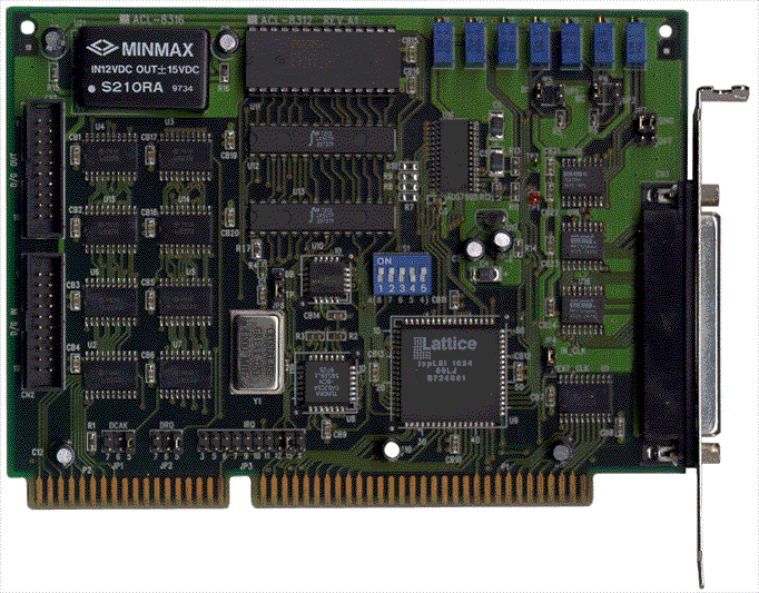
The ADLINK ACL‑8216 is a high‑performance, 16‑bit resolution, multi‑function data acquisition (DAQ) card designed for IBM PC/AT and compatible systems. It integrates analog input (A/D), analog output (D/A), digital I/O, and timer/counter functions on a single half‑size ISA card. The ACL‑8216 is part of ADLINK’s NuDAQ family, offering high‑accuracy data acquisition at low cost for industrial, laboratory, and embedded measurement applications.
### 2. Key Features
- High‑Resolution Analog Input: 16‑bit successive approximation A/D converter (ADS7805 or equivalent).
- Flexible Channel Configuration: 16 single‑ended or 8 differential analog input channels.
- Programmable Input Range: Bipolar ±10 V, ±5 V, ±2.5 V, ±1.25 V.
- Programmable Gain: ×1, ×2, ×4, ×8.
- High Sampling Rate: Up to 100 kHz for single‑channel, 20 kHz for multi‑channel multiplexed operation.
- Fast Conversion: 8 µs conversion time.
- Dual 12‑bit D/A Outputs: Two double‑buffered analog output channels (DAC7541 or equivalent).
- Selectable Output Range: 0–5 V or 0–10 V (internal reference), ±10 V (external reference).
- Digital I/O: 16 TTL‑compatible inputs and 16 TTL‑compatible outputs.
- Programmable Counter/Timer: Three 16‑bit counters (Intel 8254) with 2 MHz base clock.
- Trigger Modes: Software, programmable pacer (timer), or external pulse trigger.
- Data Transfer Options: Polling, interrupt, or DMA (channels 1 or 3).
- Interrupt Support: Selectable IRQ3, 5, 6, 7, 9, 10, 11, 12, or 15.
- Integrated DC/DC Converter: Provides stable analog power isolation.
- Compact Design: Half‑size ISA card (163 mm × 123 mm).
- Connectors: One 37‑pin D‑type and two 20‑pin IDC connectors.
- Software Support: DOS C/C++ library, Windows DLL (ACLS‑DLL2), and LabVIEW driver (ACLS‑LVIEW).
- Calibration Support: On‑board variable resistors (VRs) for A/D and D/A calibration.
### 3. Technical Specifications
Analog Input (A/D):
- Converter Type: Successive approximation (ADS7805 or equivalent)
- Resolution: 16 bits
- Channels: 16 SE or 8 DIFF
- Input Range: ±10 V, ±5 V, ±2.5 V, ±1.25 V (programmable)
- Conversion Time: 8 µs
- Sampling Rate: 100 kHz (single channel), 20 kHz (multi‑channel)
- Input Impedance: 10 MΩ / 5 pF
- Overvoltage Protection: ±35 V continuous
- Accuracy: ±1 LSB (0.003 %)
- Differential Linearity Error: ±2 LSB
- Trigger Sources: Software, pacer, external
- Data Transfer: Polling, interrupt, DMA
Analog Output (D/A):
- Converter Type: Monolithic multiplying DAC (DAC7541 or equivalent)
- Resolution: 12 bits
- Channels: 2 (double‑buffered)
- Output Range:
- Internal reference: 0–5 V or 0–10 V (unipolar)
- External reference: ±10 V max
- Settling Time: 30 µs
- Linearity: ±½ LSB
- Output Drive: ±5 mA
Digital I/O:
- Channels: 16 DI + 16 DO (TTL compatible)
- Input Voltage: Low ≤ 0.8 V, High ≥ 2.0 V
- Output Voltage: Low ≤ 0.5 V, High ≥ 2.7 V
- Drive Capability: Sink 8 mA, Source 0.4 mA
Timer/Counter (8254):
- Counters: 3 × 16‑bit programmable down counters
- Clock Source: 2 MHz internal or external (CN3 pin 37)
- Pacer Output Frequency: 0.00046 Hz – 100 kHz
- Modes: 0–5 (interrupt, one‑shot, rate generator, square wave, strobe)
General:
- I/O Base Address: 16 consecutive I/O locations (default = 0x220)
- DMA Channels: 1 or 3
- Interrupts: IRQ3, 5, 6, 7, 9, 10, 11, 12, 15
- Power Consumption: +5 V @ 420 mA max, +12 V @ 240 mA max
- Operating Temperature: 0 °C – 55 °C
- Storage Temperature: −20 °C – 80 °C
- Humidity: 5 – 95 % RH (non‑condensing)
- Dimensions: 163 mm (L) × 123 mm (W)
- Form Factor: Half‑size ISA card
### 4. Functionality
The ACL‑8216 integrates multiple data acquisition functions into a single ISA‑bus card:
- Analog Input (A/D): Converts analog signals to 16‑bit digital data. Supports single‑ended or differential inputs with programmable gain and range. Triggered by software, internal pacer, or external signal.
- Analog Output (D/A): Generates precise analog voltages from digital values. Two 12‑bit channels with double buffering ensure smooth transitions.
- Digital I/O: Provides 16 input and 16 output TTL lines for control and monitoring of external devices.
- Timer/Counter: Three 16‑bit counters for event counting, frequency generation, or pacer triggering.
- Triggering and Synchronization: Internal pacer (2 MHz base), software, or external trigger input (CN3 pin 17).
- Data Transfer: Supports CPU polling, interrupt‑driven, or DMA‑based transfer for high‑speed acquisition.
Typical Applications:
- Industrial process monitoring and control
- Laboratory instrumentation
- Automated test systems
- Signal analysis and waveform generation
- Data logging and sensor measurement
- Embedded control systems
Compatibility:
- ISA‑Bus PC/AT and compatible computers
- Supported OS: DOS, Windows 3.1/95/98/NT (via ACLS‑DLL2)
- Supported Software: C/C++, Visual C++, Visual Basic, Delphi, LabVIEW
### 5. Components & Accessories
Included Items:
- ACL‑8216 Data Acquisition Card
- ADLINK Software CD (includes DOS utilities, Windows DLLs, LabVIEW drivers, demo programs)
- User’s Manual
Connectors:
- CN1 (20‑pin IDC): Digital Output (DO0–DO15)
- CN2 (20‑pin IDC): Digital Input (DI0–DI15)
- CN3 (37‑pin D‑type): Analog I/O and Timer/Counter signals
Optional Daughter Boards:
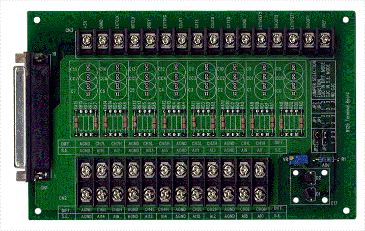
- ACLD‑8125: 37‑pin terminal board with cold‑junction compensation for thermocouples.
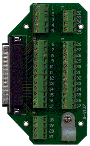
- ACLD‑9137: Direct connection board for simple analog I/O wiring.
- ACLD‑9182: 16‑channel isolated digital input board (500 V DC isolation).
- ACLD‑9185: 16‑channel SPDT relay output board.
- ACLD‑9188: General‑purpose terminal board for 37‑pin D‑sub connections.
### 6. Installation & Setup
System Requirements:
- IBM PC/AT or compatible with ISA slot
- Available I/O address range (default = 0x220)
- Available IRQ and DMA channels
Installation Steps:
1. Unpack the card using anti‑static precautions.
2. Verify no physical damage.
3. Set base I/O address via DIP switch SW1 (default 0x220).
4. Configure jumpers:
- JP3: Analog input mode (Single‑ended/Differential)
- JP7/JP8: DMA channel (1 or 3)
- JP4: Trigger source (Internal/External)
- JP6: Clock source (Internal 2 MHz/External)
- JP1/JP2: D/A reference voltage (Internal ±5 V or ±10 V, or External)
- JP7: IRQ level (default IRQ15)
5. Insert the card into an ISA slot and secure it.
6. Connect external signals to CN1, CN2, and CN3 as per pin assignments.
7. Install software from the ADLINK CD and configure drivers.
Calibration:
Five on‑board variable resistors (VR1–VR6) allow fine adjustment of A/D and D/A accuracy.
- VR1: A/D bipolar offset
- VR2: A/D full‑scale
- VR3: D/A CH1 full‑scale
- VR4: D/A CH2 full‑scale
- VR5: A/D amplifier offset
- VR6: D/A reference voltage
### 7. Performance & Capabilities
Analog Input Performance:
- 16‑bit resolution ensures high precision (1 part in 65,536).
- 8 µs conversion time supports up to 100 kS/s throughput.
- ±35 V overvoltage protection safeguards inputs.
- Programmable gain and range optimize signal‑to‑noise ratio.
Analog Output Performance:
- 12‑bit resolution with 30 µs settling time.
- Double‑buffered architecture prevents output glitches.
- ±5 mA drive capability suitable for moderate load control.
Digital I/O Performance:
- TTL‑compatible levels for direct interfacing with logic devices.
- 16 input and 16 output lines for flexible control.
Timer/Counter Performance:
- 2 MHz base clock provides fine timing resolution.
- Cascaded counters enable precise pacer frequencies from 0.00046 Hz to 100 kHz.
Limitations:
- ISA‑bus bandwidth limits maximum DMA throughput compared to modern PCI/PCIe cards.
- Single‑ended mode susceptible to ground noise in long cable runs; differential mode recommended for precision.
### 8. Standards & Compliance
- Bus Interface: ISA (AT‑Bus)
- Electrical Compatibility: TTL/DTL logic levels
- Environmental: Operating 0–55 °C, Storage −20–80 °C, 5–95 % RH non‑condensing
- Safety & EMC: Designed for industrial PC environments (no explicit CE/FCC marking in legacy documentation)
- Software Standards: Compatible with Borland C/C++, Microsoft Visual C++, Visual Basic, Delphi, and National Instruments LabVIEW
- Industry Standards: 8254 timer/counter, 8237 DMA controller, ADS7805 A/D converter, DAC7541 D/A converter
### 9. Additional Information
Software Support:
- DOS Library: C/C++ functions for A/D, D/A, DIO, and timer operations.
- Windows DLL (ACLS‑DLL2): For Windows 3.1/95/98/NT, supports VC++, VB, Delphi.
- LabVIEW Driver (ACLS‑LVIEW): Provides VIs for integration with NI LabVIEW.
- Demo Programs:
- AD_DEMO1–4: A/D conversions (software, interrupt, DMA, multi‑channel)
- DA_DEMO: D/A output
- DI_DEMO / DO_DEMO: Digital I/O
- TMR_DEMO: Timer/counter operation
Calibration Utility:
- DOS utility `8216UTIL.EXE` guides users through A/D and D/A calibration using a precision multimeter and voltage source.
Warranty:
- Duration: 1 year from date of purchase.
- Coverage: Free from defects in materials and workmanship.
- Exclusions: Damage from misuse, modification, or operation beyond specifications.
- Service: Return to ADLINK (postage prepaid) with proof of purchase for repair or replacement.
Maintenance:
- Periodic calibration recommended for high‑accuracy applications.
- Keep card free from dust and moisture; store in anti‑static packaging when not in use.
Support & Updates:
- Firmware and driver updates available via ADLINK website.
- Technical assistance provided through dedicated NuDAQ support channels.
### Summary
The ADLINK ACL‑8216 is a robust, high‑resolution, multi‑function data acquisition card engineered for ISA‑bus PCs. It combines 16‑bit analog input, 12‑bit analog output, digital I/O, and timer/counter capabilities in a compact form factor. With flexible triggering, DMA and interrupt data transfer, and comprehensive software support, it serves as a versatile platform for industrial automation, laboratory measurement, and embedded control systems. Its precision, configurability, and reliability make it a proven solution for legacy and specialized data acquisition applications requiring deterministic performance and direct hardware control.

### 1. Product Overview
Product Name: ACL‑8216
Model: ACL‑8216
Series: NuDAQ ISA‑Bus Data Acquisition Series
Article Number: ACL‑8216
Manufacturer: ADLINK Technology Inc.
Manufacturer Address: 9F, No. 166, Jian Yi Road, Chungho City, Taipei 235, Taiwan, R.O.C.
Website: [www.adlink.com.tw](http://www.adlink.com.tw)
Support Contacts:
- Sales & Service: service@adlink.com.tw
- Technical Support (NuDAQ): nudaq@adlink.com.tw
- Software Support: sw@adlink.com.tw
- Telephone: +886‑2‑82265877
- Fax: +886‑2‑82265717
The ADLINK ACL‑8216 is a high‑performance, 16‑bit resolution, multi‑function data acquisition (DAQ) card designed for IBM PC/AT and compatible systems. It integrates analog input (A/D), analog output (D/A), digital I/O, and timer/counter functions on a single half‑size ISA card. The ACL‑8216 is part of ADLINK’s NuDAQ family, offering high‑accuracy data acquisition at low cost for industrial, laboratory, and embedded measurement applications.
### 2. Key Features
- High‑Resolution Analog Input: 16‑bit successive approximation A/D converter (ADS7805 or equivalent).
- Flexible Channel Configuration: 16 single‑ended or 8 differential analog input channels.
- Programmable Input Range: Bipolar ±10 V, ±5 V, ±2.5 V, ±1.25 V.
- Programmable Gain: ×1, ×2, ×4, ×8.
- High Sampling Rate: Up to 100 kHz for single‑channel, 20 kHz for multi‑channel multiplexed operation.
- Fast Conversion: 8 µs conversion time.
- Dual 12‑bit D/A Outputs: Two double‑buffered analog output channels (DAC7541 or equivalent).
- Selectable Output Range: 0–5 V or 0–10 V (internal reference), ±10 V (external reference).
- Digital I/O: 16 TTL‑compatible inputs and 16 TTL‑compatible outputs.
- Programmable Counter/Timer: Three 16‑bit counters (Intel 8254) with 2 MHz base clock.
- Trigger Modes: Software, programmable pacer (timer), or external pulse trigger.
- Data Transfer Options: Polling, interrupt, or DMA (channels 1 or 3).
- Interrupt Support: Selectable IRQ3, 5, 6, 7, 9, 10, 11, 12, or 15.
- Integrated DC/DC Converter: Provides stable analog power isolation.
- Compact Design: Half‑size ISA card (163 mm × 123 mm).
- Connectors: One 37‑pin D‑type and two 20‑pin IDC connectors.
- Software Support: DOS C/C++ library, Windows DLL (ACLS‑DLL2), and LabVIEW driver (ACLS‑LVIEW).
- Calibration Support: On‑board variable resistors (VRs) for A/D and D/A calibration.
### 3. Technical Specifications
Analog Input (A/D):
- Converter Type: Successive approximation (ADS7805 or equivalent)
- Resolution: 16 bits
- Channels: 16 SE or 8 DIFF
- Input Range: ±10 V, ±5 V, ±2.5 V, ±1.25 V (programmable)
- Conversion Time: 8 µs
- Sampling Rate: 100 kHz (single channel), 20 kHz (multi‑channel)
- Input Impedance: 10 MΩ / 5 pF
- Overvoltage Protection: ±35 V continuous
- Accuracy: ±1 LSB (0.003 %)
- Differential Linearity Error: ±2 LSB
- Trigger Sources: Software, pacer, external
- Data Transfer: Polling, interrupt, DMA
Analog Output (D/A):
- Converter Type: Monolithic multiplying DAC (DAC7541 or equivalent)
- Resolution: 12 bits
- Channels: 2 (double‑buffered)
- Output Range:
- Internal reference: 0–5 V or 0–10 V (unipolar)
- External reference: ±10 V max
- Settling Time: 30 µs
- Linearity: ±½ LSB
- Output Drive: ±5 mA
Digital I/O:
- Channels: 16 DI + 16 DO (TTL compatible)
- Input Voltage: Low ≤ 0.8 V, High ≥ 2.0 V
- Output Voltage: Low ≤ 0.5 V, High ≥ 2.7 V
- Drive Capability: Sink 8 mA, Source 0.4 mA
Timer/Counter (8254):
- Counters: 3 × 16‑bit programmable down counters
- Clock Source: 2 MHz internal or external (CN3 pin 37)
- Pacer Output Frequency: 0.00046 Hz – 100 kHz
- Modes: 0–5 (interrupt, one‑shot, rate generator, square wave, strobe)
General:
- I/O Base Address: 16 consecutive I/O locations (default = 0x220)
- DMA Channels: 1 or 3
- Interrupts: IRQ3, 5, 6, 7, 9, 10, 11, 12, 15
- Power Consumption: +5 V @ 420 mA max, +12 V @ 240 mA max
- Operating Temperature: 0 °C – 55 °C
- Storage Temperature: −20 °C – 80 °C
- Humidity: 5 – 95 % RH (non‑condensing)
- Dimensions: 163 mm (L) × 123 mm (W)
- Form Factor: Half‑size ISA card
### 4. Functionality
The ACL‑8216 integrates multiple data acquisition functions into a single ISA‑bus card:
- Analog Input (A/D): Converts analog signals to 16‑bit digital data. Supports single‑ended or differential inputs with programmable gain and range. Triggered by software, internal pacer, or external signal.
- Analog Output (D/A): Generates precise analog voltages from digital values. Two 12‑bit channels with double buffering ensure smooth transitions.
- Digital I/O: Provides 16 input and 16 output TTL lines for control and monitoring of external devices.
- Timer/Counter: Three 16‑bit counters for event counting, frequency generation, or pacer triggering.
- Triggering and Synchronization: Internal pacer (2 MHz base), software, or external trigger input (CN3 pin 17).
- Data Transfer: Supports CPU polling, interrupt‑driven, or DMA‑based transfer for high‑speed acquisition.
Typical Applications:
- Industrial process monitoring and control
- Laboratory instrumentation
- Automated test systems
- Signal analysis and waveform generation
- Data logging and sensor measurement
- Embedded control systems
Compatibility:
- ISA‑Bus PC/AT and compatible computers
- Supported OS: DOS, Windows 3.1/95/98/NT (via ACLS‑DLL2)
- Supported Software: C/C++, Visual C++, Visual Basic, Delphi, LabVIEW
### 5. Components & Accessories
Included Items:
- ACL‑8216 Data Acquisition Card
- ADLINK Software CD (includes DOS utilities, Windows DLLs, LabVIEW drivers, demo programs)
- User’s Manual
Connectors:
- CN1 (20‑pin IDC): Digital Output (DO0–DO15)
- CN2 (20‑pin IDC): Digital Input (DI0–DI15)
- CN3 (37‑pin D‑type): Analog I/O and Timer/Counter signals
Optional Daughter Boards:
- ACLD‑8125: 37‑pin terminal board with cold‑junction compensation for thermocouples.
- ACLD‑9137: Direct connection board for simple analog I/O wiring.
- ACLD‑9182: 16‑channel isolated digital input board (500 V DC isolation).
- ACLD‑9185: 16‑channel SPDT relay output board.
- ACLD‑9188: General‑purpose terminal board for 37‑pin D‑sub connections.
### 6. Installation & Setup
System Requirements:
- IBM PC/AT or compatible with ISA slot
- Available I/O address range (default = 0x220)
- Available IRQ and DMA channels
Installation Steps:
1. Unpack the card using anti‑static precautions.
2. Verify no physical damage.
3. Set base I/O address via DIP switch SW1 (default 0x220).
4. Configure jumpers:
- JP3: Analog input mode (Single‑ended/Differential)
- JP7/JP8: DMA channel (1 or 3)
- JP4: Trigger source (Internal/External)
- JP6: Clock source (Internal 2 MHz/External)
- JP1/JP2: D/A reference voltage (Internal ±5 V or ±10 V, or External)
- JP7: IRQ level (default IRQ15)
5. Insert the card into an ISA slot and secure it.
6. Connect external signals to CN1, CN2, and CN3 as per pin assignments.
7. Install software from the ADLINK CD and configure drivers.
Calibration:
Five on‑board variable resistors (VR1–VR6) allow fine adjustment of A/D and D/A accuracy.
- VR1: A/D bipolar offset
- VR2: A/D full‑scale
- VR3: D/A CH1 full‑scale
- VR4: D/A CH2 full‑scale
- VR5: A/D amplifier offset
- VR6: D/A reference voltage
### 7. Performance & Capabilities
Analog Input Performance:
- 16‑bit resolution ensures high precision (1 part in 65,536).
- 8 µs conversion time supports up to 100 kS/s throughput.
- ±35 V overvoltage protection safeguards inputs.
- Programmable gain and range optimize signal‑to‑noise ratio.
Analog Output Performance:
- 12‑bit resolution with 30 µs settling time.
- Double‑buffered architecture prevents output glitches.
- ±5 mA drive capability suitable for moderate load control.
Digital I/O Performance:
- TTL‑compatible levels for direct interfacing with logic devices.
- 16 input and 16 output lines for flexible control.
Timer/Counter Performance:
- 2 MHz base clock provides fine timing resolution.
- Cascaded counters enable precise pacer frequencies from 0.00046 Hz to 100 kHz.
Limitations:
- ISA‑bus bandwidth limits maximum DMA throughput compared to modern PCI/PCIe cards.
- Single‑ended mode susceptible to ground noise in long cable runs; differential mode recommended for precision.
### 8. Standards & Compliance
- Bus Interface: ISA (AT‑Bus)
- Electrical Compatibility: TTL/DTL logic levels
- Environmental: Operating 0–55 °C, Storage −20–80 °C, 5–95 % RH non‑condensing
- Safety & EMC: Designed for industrial PC environments (no explicit CE/FCC marking in legacy documentation)
- Software Standards: Compatible with Borland C/C++, Microsoft Visual C++, Visual Basic, Delphi, and National Instruments LabVIEW
- Industry Standards: 8254 timer/counter, 8237 DMA controller, ADS7805 A/D converter, DAC7541 D/A converter
### 9. Additional Information
Software Support:
- DOS Library: C/C++ functions for A/D, D/A, DIO, and timer operations.
- Windows DLL (ACLS‑DLL2): For Windows 3.1/95/98/NT, supports VC++, VB, Delphi.
- LabVIEW Driver (ACLS‑LVIEW): Provides VIs for integration with NI LabVIEW.
- Demo Programs:
- AD_DEMO1–4: A/D conversions (software, interrupt, DMA, multi‑channel)
- DA_DEMO: D/A output
- DI_DEMO / DO_DEMO: Digital I/O
- TMR_DEMO: Timer/counter operation
Calibration Utility:
- DOS utility `8216UTIL.EXE` guides users through A/D and D/A calibration using a precision multimeter and voltage source.
Warranty:
- Duration: 1 year from date of purchase.
- Coverage: Free from defects in materials and workmanship.
- Exclusions: Damage from misuse, modification, or operation beyond specifications.
- Service: Return to ADLINK (postage prepaid) with proof of purchase for repair or replacement.
Maintenance:
- Periodic calibration recommended for high‑accuracy applications.
- Keep card free from dust and moisture; store in anti‑static packaging when not in use.
Support & Updates:
- Firmware and driver updates available via ADLINK website.
- Technical assistance provided through dedicated NuDAQ support channels.
### Summary
The ADLINK ACL‑8216 is a robust, high‑resolution, multi‑function data acquisition card engineered for ISA‑bus PCs. It combines 16‑bit analog input, 12‑bit analog output, digital I/O, and timer/counter capabilities in a compact form factor. With flexible triggering, DMA and interrupt data transfer, and comprehensive software support, it serves as a versatile platform for industrial automation, laboratory measurement, and embedded control systems. Its precision, configurability, and reliability make it a proven solution for legacy and specialized data acquisition applications requiring deterministic performance and direct hardware control.
-
A8216 Manual.PDF
Manual
- ACLD-8125 - Panel with cold junction compensation
- ACLD-9138-01 - Panel general purpose, 2*20 small screw terminal
- ACLD-9137-01 - Direct 37 small screw terminal
- DIN-37D-01 - 37pin D-type panel DIN rail w/o cable
- ACLD-9182A-01 - isolated 16 DI (DC) panel
- ACLD-9185-01 - isolated 16 DO Relay panel
- ACLD-9188 - Panel for mounting low pass filter etc.
- DIN-20P-01 - 20pin header termination board DIN rail
- ACL-10337 - 2*20 pin to DB 37 slot adapter