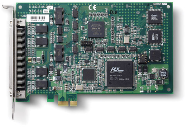
Comprehensive Product Summary – ADLINK PCIe‑7350 High‑Speed Digital I/O Card
### 1. Product Overview
Product Name: PCIe‑7350
Model: PCIe‑7350
Series: ADLINK PCI Express® High‑Speed Digital I/O Series
Article Number: PCIe‑7350
Manufacturer: ADLINK Technology Inc.
Product Type: 32‑Channel High‑Speed Digital Input/Output (DIO) PCI Express® Card
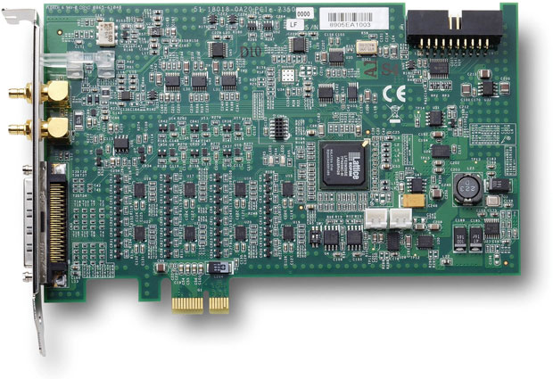
Description: The ADLINK PCIe‑7350 is a high‑performance, 32‑channel, bi‑directional digital I/O card designed for high‑speed data acquisition, pattern generation, and digital communication applications. It supports up to 200 MB/s data throughput via a PCI Express® x1 interface and offers flexible logic‑level configuration, advanced triggering, and programmable serial interfaces (I²C/SPI).
### 2. Key Features
- High‑Speed PCI Express® Interface:
- x1 lane PCI Express® interface delivering up to 200 MB/s maximum throughput.
- Bus‑mastering DMA with scatter‑gather support for efficient, CPU‑independent data transfer.
- Flexible Clocking Architecture:
- Internal clock up to 50 MHz (programmable divider 100 MHz/N, 2 ≤ N ≤ 65,535).
- External clock up to 100 MHz (supports 8/16‑bit data width).
- 16‑step phase shift (22.5° increments) for precise timing alignment.
- Programmable Logic Levels:
- Software‑selectable logic levels: 1.8 V, 2.5 V, or 3.3 V (5 V compatible).
- Uniform logic level applied across all I/O groups.
- Configurable I/O Direction:
- 32 bi‑directional channels divided into four 8‑bit groups (A–D).
- Each group independently configurable as input or output.
- Advanced Triggering and Handshaking:
- Supports software, external digital, pattern match, post/re‑trigger, and gated trigger modes.
- Flexible handshaking (DI‑REQ/DI‑ACK, DO‑REQ/DO‑ACK) and burst handshaking for reliable data exchange.
- Auxiliary Function I/O (AFI):
- 8 programmable AFI channels configurable for I²C, SPI, trigger, event, or clock I/O.
- I²C master (up to 244 kHz) and SPI master (up to 62.5 MHz) support.
- High‑Speed Data Integrity:
- 8 K‑sample FIFO buffers for both input and output.
- Scatter‑gather DMA ensures continuous, loss‑free data streaming.
- Software and OS Support:
- Compatible with Windows 2000/XP/Vista/2003.
- Supported programming environments: VB.NET, VC.NET, Delphi, BCB, DAQBench.
- Driver package: PCIS‑DASK for Windows.
### 3. Technical Specifications
Digital I/O:
- Channels: 32 bi‑directional (4 × 8‑bit groups).
- Logic Levels: 1.8 V / 2.5 V / 3.3 V (software selectable, 5 V tolerant).
- Input Impedance: 10 kΩ.
- Output Impedance: 50 Ω.
- Input Protection: −1 V to +6 V.
- Output Protection: −0.5 V to +3.8 V.
- Power‑Up State: All channels default to input (tri‑state outputs).
Voltage Thresholds:
| Parameter | 1.8 V | 2.5 V | 3.3 V |
|------------|--------|--------|--------|
| Min VIH | 1.2 V | 1.6 V | 2.0 V |
| Max VIL | 0.63 V | 0.7 V | 0.8 V |
| Min VOH | 1.6 V | 2.3 V | 3.1 V |
| Max VOL | 0.2 V | 0.2 V | 0.2 V |
| Max Drive Current | ±8 mA | ±16 mA | ±32 mA |
Performance:
- Maximum Throughput: 200 MB/s (32‑bit @ 50 MHz).
- Sustained Throughput:
- DI: 192 MB/s (data > 250 k samples).
- DO: 119 MB/s sustained, 200 MB/s peak (≤ 8 K samples).
- FIFO Size: 8 K samples (DI + DO).
- Clock Jitter: 160 ps period jitter.
- Channel‑to‑Channel Skew: ±1.08 ns.
Timing Accuracy:
- Setup Time (tSU): 2 ns
- Hold Time (tH): 2 ns
- External Clock Delay (AFI7 → internal): 7.22 ns
- External Clock Delay (SMB IN → internal): 8.02 ns
Physical Characteristics:
- Dimensions: 168 mm (L) × 112 mm (H) (excluding connectors).
- Connectors: 1 × 68‑pin VHDCI female, 2 × SMB jacks (CLK IN/OUT).
- Weight: Approx. 200 g (typical board only).
- Power Consumption: +3.3 V @ 780 mA max, +12 V @ 680 mA max (≈ 10.8 W).
Environmental:
- Operating Temperature: 0 °C to 55 °C.
- Storage Temperature: −20 °C to 70 °C.
- Humidity: 5 % to 95 %, non‑condensing.
### 4. Functionality
Operating Principle:
The PCIe‑7350 provides 32 bi‑directional digital lines grouped into four 8‑bit ports. Each port can be independently configured for input or output. Data transfer occurs via bus‑mastering DMA, enabling high‑speed, low‑latency communication between the card and system memory without CPU overhead.
Clocking:
- Internal 100 MHz oscillator with programmable divider.
- External clock input via SMB IN or AFI6/AFI7.
- Exportable clock output via SMB OUT or AFI6/AFI7.
- 16‑step phase shift (22.5° increments) for timing optimization.
Use Cases & Applications:
- High‑speed digital data acquisition and playback.
- IC and semiconductor device testing.
- Automated Test Equipment (ATE).
- Digital pattern generation and verification.
- Interface to high‑speed ADC/DAC modules.
- Image sensor or video data capture.
- Real‑time digital communication emulation.
Compatibility:
- PCI Express® x1 slot (compatible with x4/x8/x16 slots).
- Works with ADLINK DIN‑68H terminal board and ACL‑10279 VHDCI cable.
### 5. Components & Accessories
Included Items:
- PCIe‑7350 card.
- ADLINK All‑in‑One CD (software drivers and manuals).
- Printed User Manual.
Optional Accessories:
- DIN‑68H‑01: 68‑pin SCSI‑VHDCI terminal board with 0 Ω or 50 Ω selectable impedance.
- ACL‑10279: 68‑pin SCSI‑VHDCI cable (50 Ω impedance).
- SMB‑SMB‑1M: 1 m SMB‑to‑SMB cable for clock I/O.
- SMB‑BNC‑1M: 1 m SMB‑to‑BNC cable for external clock connections.
Connectors:
- CN1 (68‑pin VHDCI): 32 data lines (D0–D31), 8 AFI lines (AF0–AF7), and ground pins.
- CN2/CN3 (SMB Jacks): CLK IN and CLK OUT for external clock synchronization.
### 6. Installation & Setup
System Requirements:
- Available PCI Express® x1 slot.
- Windows 2000/XP/Vista/2003 operating system.
- Administrator privileges for driver installation.
Installation Steps:
1. Install the ADLINK driver (PCIS‑DASK) before inserting the card.
2. Power off the system and remove the chassis cover.
3. Insert the PCIe‑7350 into an available PCIe slot and secure it.
4. Reassemble the system and power on.
5. Verify installation via Device Manager or ADLINK diagnostic tools.
Configuration:
- No jumper settings required; all resources (IRQ, DMA, base address) are auto‑assigned by the system BIOS.
- Logic level and I/O direction are software‑configurable per group.
Mounting Options:
- Standard PCIe bracket for desktop chassis.
- Compatible with DIN‑68H terminal board for bench testing and signal termination.
### 7. Performance & Capabilities
Data Transfer:
- Bus‑Mastering DMA: Direct memory access without CPU intervention.
- Scatter‑Gather DMA: Supports non‑contiguous memory blocks for large data sets.
- FIFO Buffering: 8 K samples each for input and output to prevent data loss.
Clocking & Timing:
- Internal clock range: 1.5 kHz to 50 MHz.
- External clock range: 100 kHz to 100 MHz (phase shift enabled 2–50 MHz).
- Exported clock frequency: 0–50 MHz (phase shift enabled 2–50 MHz).
Triggering:
- Sources: Software command or external digital signal (AF0–AF7).
- Modes: Post trigger, re‑trigger, gated trigger, pattern match.
- Change‑of‑State Interrupt: Detects any state change on selected channels.
Handshaking:
- DI Mode: DI‑REQ (input) and DI‑ACK (output).
- DO Mode: DO‑REQ (output) and DO‑ACK (input).
- Burst Handshaking: Combines continuous and handshake modes for optimized throughput.
Auxiliary Functions:
- I²C Master: SCL (AF0), SDA (AF1); 1.9 kHz – 244 kHz clock.
- SPI Master: SCK (AF0), SDO (AF1), SDI (AF2), CS0–CS2 (AF3–AF5); 244 kHz – 62.5 MHz.
- Event Outputs: Pattern Match (PM) and Change‑of‑State (COS) events with programmable pulse width (8 ns – 34.36 s).
Limitations:
- External clock > 50 MHz not supported for phase shift operation.
- DO throughput limited to 8 K FIFO size for 200 MB/s peak rate.
- Logic level selection applies globally to all I/O groups.
### 8. Standards & Compliance
- Interface Standard: PCI Express® Base Specification Revision 1.0 (x1 lane).
- Electrical Compliance: Meets PCIe signal integrity and EMC requirements.
- Safety and Environmental: Designed for industrial use (0–55 °C operation).
- RoHS Compliance: Lead‑free manufacturing process.
- Software API: PCIS‑DASK library for Windows 98/NT/2000/XP/Vista.
### 9. Additional Information
Warranty & Support:
- Standard ADLINK limited hardware warranty (typically 2 years).
- Global technical support via regional offices (Taiwan, USA, China, Japan, Europe, Singapore, India, Korea).
- Email support: service@adlinktech.com / info@adlinktech.com.
Maintenance:
- Handle with anti‑static precautions.
- Avoid exposure to moisture and excessive heat.
- Periodic connector inspection recommended for high‑frequency applications.
Software Updates:
- Driver and firmware updates available from [www.adlinktech.com](https://www.adlinktech.com).
- PCIS‑DASK API provides continuous support for new Windows versions.
Ordering Information:
- PCIe‑7350: 32‑CH High‑Speed DIO PCI Express® Card.
- DIN‑68H‑01: 68‑pin Terminal Board (0 Ω / 50 Ω Selectable Impedance).
- ACL‑10279: 68‑pin VHDCI Cable (50 Ω).
- SMB‑SMB‑1M: 1 m SMB Cable.
### Summary
The ADLINK PCIe‑7350 is a robust, high‑speed digital I/O solution engineered for demanding test, measurement, and automation environments. Its combination of 200 MB/s throughput, programmable logic levels, flexible triggering, and I²C/SPI integration makes it ideal for applications requiring precise digital pattern control and synchronization. With comprehensive software support, scatter‑gather DMA, and advanced timing features, the PCIe‑7350 delivers deterministic, high‑integrity digital data transfer for industrial and research systems alike.



 SUCHEN SIE DIE PASSENDE
 PCIe-7350_Datasheet_3.pdf
PDF Catalog
PCIe-7350_Datasheet_3.pdf
PDF Catalog