Comprehensive Product Summary – ADLINK ACL‑8316 High‑Performance Data Acquisition Card
### 1. Product Overview
Product Name: ACL‑8316
Model: ACL‑8316
Series: ACL‑8316/8312 High‑Performance DAS (Data Acquisition System) Cards
Article Number: ACL‑8316
Manufacturer: ADLINK Technology Inc.
Trademark: NuDAQ® (registered trademark of ADLINK Technology Inc.)
Product Type: Multifunction Analog and Digital I/O Data Acquisition Card for PC/ISA Bus Systems
Form Factor: Half‑size ISA card (163 mm × 123 mm)
Country of Origin: Taiwan, R.O.C.
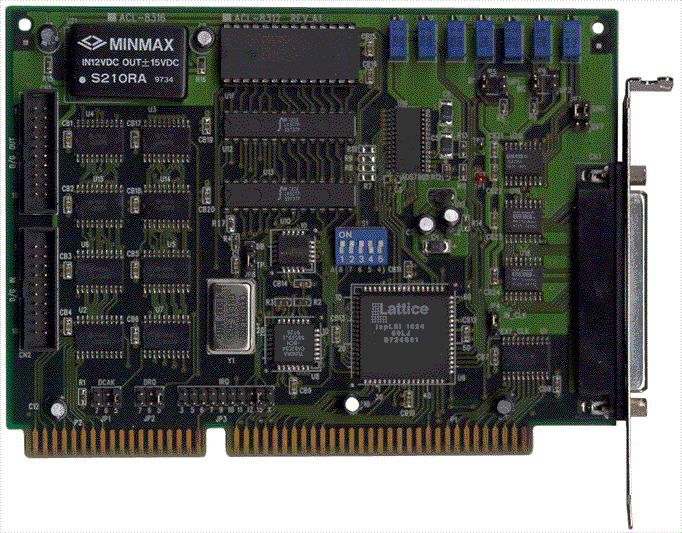
The ADLINK ACL‑8316 is a high‑resolution, high‑performance data acquisition (DAQ) card designed for PC/ISA bus architecture. It provides 16‑bit analog‑to‑digital conversion, dual 12‑bit analog outputs, 16 digital I/O lines, and three programmable 16‑bit counters. The card integrates a 1K‑word FIFO buffer, DMA transfer capability, and multiple trigger modes for continuous, gap‑free data acquisition. It is ideal for industrial measurement, control, and laboratory automation applications.
### 2. Key Features
- High‑Resolution Analog Input: 16‑bit A/D conversion (ADS7805 or equivalent) with up to 100 kS/s sampling rate.
- Flexible Channel Configuration: 16 single‑ended or 8 differential analog input channels.
- Programmable Gain: x1, x2, x4, x8 for input ranges of ±10 V, ±5 V, ±2.5 V, ±1.25 V.
- On‑Board FIFO Buffer: 1K‑word FIFO memory with half‑ and full‑ready interrupt flags for continuous data streaming.
- Dual Analog Outputs: Two 12‑bit D/A channels (DAC2813 or equivalent) with bipolar/unipolar ranges (±10 V or 0–10 V).
- Digital I/O: 16 TTL‑compatible digital input and 16 digital output channels.
- Programmable Counter/Timer: Three independent 16‑bit down counters (Intel 8254 compatible) with 2 MHz base clock.
- Trigger Flexibility: Software, internal pacer, and external trigger modes.
- DMA and Interrupt Support: DMA channels 5, 6, or 7; IRQ levels 3, 5–7, 9, 11, 12, 15.
- Auto‑Scanning: Hardware channel auto‑scan for sequential sampling.
- Integrated DC/DC Converter: Provides stable analog power isolation.
- Compact Design: Half‑size ISA card with 37‑pin D‑type and dual 20‑pin IDC connectors.
- Software Support: C/C++ library, DOS utilities, Windows DLL (ACLS‑DLL2), and LabVIEW driver (ACLS‑LVIEW).
- Calibration Support: On‑board variable resistors (VR1–VR7) for A/D and D/A calibration.
### 3. Technical Specifications
Analog Input (A/D):
- Converter: Burr‑Brown ADS7805 (ACL‑8316)
- Resolution: 16 bits
- Channels: 16 SE or 8 DI
- Conversion Type: Successive approximation
- Conversion Time: 8 µs
- Max Sampling Rate: 100 kS/s
- Input Range: ±10 V, ±5 V, ±2.5 V, ±1.25 V (programmable)
- Input Impedance: 10 MΩ
- Accuracy:
- Gain 1: 0.01% FSR ±1 LSB
- Gain 2/4: 0.02% FSR ±1 LSB
- Gain 8: 0.04% FSR ±1 LSB
- Overvoltage Protection: ±35 V continuous
- Data Format: Two’s complement
- FIFO Memory: 1K words
- Trigger Modes: Software, internal pacer, external pulse
- Data Transfer: Polling, interrupt, FIFO, DMA
Analog Output (D/A):
- Converter: DAC2813 or equivalent
- Resolution: 12 bits
- Channels: 2
- Output Range: ±10 V (bipolar) or 0–10 V (unipolar)
- Settling Time: 4.5 µs typical, 6 µs max
- Output Drive: ±5 mA min
- Output Impedance: 0.2 Ω
- Linearity: ±½ LSB max
- Modes: Double‑buffered or transparent
- Data Format: Binary or two’s complement
Digital I/O:
- Channels: 16 input, 16 output (TTL compatible)
- Input Voltage: Low ≤ 0.8 V, High ≥ 2.0 V
- Output Voltage: Low ≤ 0.4 V, High ≥ 2.4 V
- Drive Capacity: Sink 8 mA @ 0.5 V, Source 0.4 mA @ 2.7 V
Counter/Timer:
- Device: Intel 82C54 compatible
- Counters: 3 × 16‑bit
- Base Clock: 2 MHz
- Pacer Output Range: 0.00046 Hz – 100 kHz
- Modes: 0–5 (interrupt, one‑shot, rate generator, square wave, strobe)
General:
- Bus Interface: 16‑bit ISA
- I/O Base Address: 16 consecutive locations (default 0x220)
- IRQ Levels: 3, 5, 6, 7, 9, 11, 12, 15
- DMA Channels: 5, 6, 7
- Power Requirements: +5 V @ 400 mA, +12 V @ 260 mA
- Operating Temperature: 0–55 °C
- Storage Temperature: –20–80 °C
- Humidity: 5–95% non‑condensing
- Dimensions: 163 mm (L) × 123 mm (H)
### 4. Functionality
The ACL‑8316 performs high‑speed analog and digital data acquisition through its integrated A/D and D/A subsystems.
Operation Principles:
- A/D Conversion: Successive approximation with programmable gain and selectable input mode (SE or DI).
- Triggering: Supports software, internal pacer (timer‑based), and external trigger via CN3 pin 17.
- Data Buffering: 1K FIFO enables continuous sampling without data loss.
- Data Transfer: Supports software polling, interrupt‑driven, FIFO half‑full interrupt, and DMA transfer for high throughput.
- D/A Conversion: Two 12‑bit channels output analog voltages in real time or synchronized double‑buffered mode.
- Digital I/O: TTL‑compatible lines for control, monitoring, or external device interfacing.
- Timer/Counter: Three programmable counters for event counting, frequency generation, or pacer timing.
Applications:
- Industrial process control and automation
- Laboratory data logging and signal analysis
- Energy management and monitoring systems
- Product testing and quality assurance
- Security and annunciation systems
- Pulse width and period measurement
Compatibility:
- PC/ISA bus systems
- Supported OS: DOS, Windows 3.1/95/98/NT
- Software Environments: C/C++, Visual C++, Visual Basic, Delphi, LabVIEW
### 5. Components & Accessories
Included Items:
- ACL‑8316 Data Acquisition Card
- ADLINK Software CD (utilities, drivers, libraries)
- User’s Manual
Connectors:
- CN1: 20‑pin IDC for digital output (DO0–DO15)
- CN2: 20‑pin IDC for digital input (DI0–DI15)
- CN3: 37‑pin D‑type for analog I/O and timer/counter signals
Optional Daughter Boards:
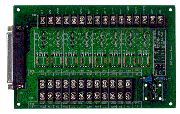
- ACLD‑8125: 37‑pin D‑sub with cold junction compensation (CJC) for thermocouple input.
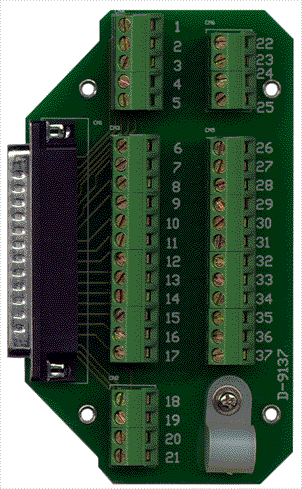
- ACLD‑9137: Direct 37‑pin connector board for simple analog signal connection.
- ACLD‑9182: 16‑channel isolated digital input board (500 VDC isolation).
- ACLD‑9185: 16‑channel SPDT relay output board for external device control.
- ACLD‑9188 / ACLD‑9138: Terminal boards with barrier‑strip or screw‑clamp terminals for general wiring.
### 6. Installation & Setup
Requirements:
- IBM‑compatible PC with available ISA slot
- Proper grounding and anti‑static precautions during installation
Configuration Options:
- Base Address: DIP switch SW1 (default 0x220, range 0x200–0x3FF)
- Analog Input Mode: JP7 selects SE (16 ch) or DI (8 ch)
- Analog Output Range: JP5 (CH1) and JP6 (CH2) select ±10 V or 0–10 V
- Output Mode: JP8 selects double‑buffered or transparent
- DMA Channel: JP1/JP2 select DMA 5, 6, or 7
- IRQ Level: JP3 selects IRQ 3, 5–7, 9, 11, 12, or 15 (default IRQ15)
- Clock Source: JP4 selects internal 2 MHz or external clock (CN3 pin 37)
Mounting:
- Insert card into ISA slot, secure bracket, connect external cables to CN1–CN3.
Software Setup:
- Install ADLINK CD software package.
- Configure base address and IRQ/DMA settings via utility.
- Use provided C/C++ library or Windows DLL for programming.
### 7. Performance & Capabilities
- A/D Sampling Rate: Up to 100 kS/s continuous.
- A/D Resolution: 16 bits, ±10 V full scale.
- D/A Update Rate: 6 µs max settling time.
- FIFO Buffer: 1K samples (10 ms at 100 kS/s).
- DMA Throughput: Real‑time transfer without CPU overhead.
- Timer Resolution: 0.5 µs (2 MHz base).
- Digital I/O Switching: TTL‑level, 16 inputs and 16 outputs.
- Accuracy: ±0.01% FSR typical at gain 1.
- Limitations: ISA bus bandwidth; single‑card DMA channel limitation (max three cards per system).
### 8. Standards & Compliance
- Bus Interface: 16‑bit ISA standard
- Timer/Counter: Intel 8254 compatible
- DMA Controller: Intel 8237 compatible
- A/D Converter: Burr‑Brown ADS7805 (industry standard)
- D/A Converter: Burr‑Brown DAC2813
- Digital Logic: TTL/DTL compatible
- Environmental Compliance: Operating 0–55 °C, 5–95% RH non‑condensing
- Electrical Safety: ±35 V overvoltage protection on analog inputs
- Software Standards: Compatible with Windows and LabVIEW environments
- Regulatory: Designed to meet industrial PC/ISA electrical and EMC standards (per ADLINK manufacturing practices)
### 9. Additional Information
Calibration:
- Seven variable resistors (VR1–VR7) for fine adjustment:
- VR1: A/D offset
- VR2: A/D full scale
- VR3/VR4: D/A CH1 full scale and offset
- VR5/VR6: D/A CH2 full scale and offset
- VR7: A/D amplifier offset
- Calibration utility software included for guided adjustment using a precision DVM and voltage calibrator.
Maintenance:
- Periodic calibration recommended for optimal accuracy.
- Handle with ESD protection; avoid exposure to high humidity or temperature extremes.
Warranty:
- One‑year limited warranty from date of purchase.
- Covers defects in materials and workmanship.
- Excludes damage from misuse, modification, or operation beyond specifications.
- Return shipping prepaid; proof of purchase required.
Technical Support:
- ADLINK Technology Inc.
- Address: 9F, No. 166, Jian Yi Road, Chungho City, Taipei 235, Taiwan
- Tel: +886‑2‑82265877
- Fax: +886‑2‑82265717
- Web: [www.adlink.com.tw](http://www.adlink.com.tw)
- Email: service@adlink.com.tw (sales/service), nudaq@adlink.com.tw (technical)
Software Updates:
- ADLINK provides updated drivers and libraries via official website.
- Supported environments include DOS, Windows 95/98/NT, and LabVIEW.
### Summary
The ADLINK ACL‑8316 is a robust, high‑precision ISA‑bus data acquisition card engineered for demanding industrial and laboratory applications. With 16‑bit analog input resolution, dual 12‑bit analog outputs, 16 digital I/O lines, and integrated timers and counters, it delivers comprehensive measurement and control capabilities. Its 1K FIFO buffer, DMA support, and multiple trigger modes enable high‑speed, gap‑free data collection. The card’s flexible configuration, software support, and calibration utilities make it a versatile solution for engineers and system integrators requiring reliable, high‑accuracy data acquisition in PC‑based systems.

 LOOKING FOR THE RIGHT
 A8316&12 Manual.PDF
Manual
A8316&12 Manual.PDF
Manual